


Users Manual TOPAS900 Flash V2.1
HWU Elektronik Oberhausen Page 14
Please refer to the memory maps to get information about the address range of the chip in
memory.
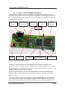
3.2.3. 128 kb RAM - Toshiba TC551001 (70 ns)
This memory component is soldered on the bottom side of the PCB. It has a size of 128
kb and is organized in 8-bit words. It is addressed by 17 address lines A0..16. The data
lines are D0..D7 and the chip is selected by /CS0 pin of the MCU. The type of operation is
selected by the /WR and /RD line accordingly.
Please refer to the memory maps to get information about the address range of the chip in
memory. The external RAM is used additionally to the internal RAM of 8 kb of the MCU.
When the Toshiba ROM monitor is running almost 32 kb are allocated to the ROM
monitor. For all monitor operations the RAM is mapped to address 0xFE0000..0xFFFFFF
and covers the interrupt vector area that must be writable for debugging purposes.
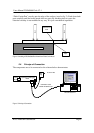
3.2.4. Connector to Programming and Debugging Board
To connect the Programming and Debugging Board a 10-pin connector is mounted at the
edge of the board. The 10-pin cable is to be plugged in on both sides to connect both
boards together.
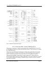
3.2.5. MCU Terminal Connectors
The Flash Carrier Board can be used - when properly programmed - stand-alone in a
user’s application. For this kind of usage it is necessary to insert and solder four 26-pin
connectors into the prepared drill holes. The prepared space for the connectors can easily
found by searching the Flash Carrier Board for the printed labels “MCU1”, “MCU2”,
“MCU3” and “MCU4”. The connections to the MCU are made as easy as possible. Each
of the 100 pins of the MCU are connected directly to MCU connectors. E.g. pin 11 of the
MCU is wired with pin11 of “MCU1” connector. Pin 26 of each connector is left out and
not connected (the MCU has 100 pins, but 4x26=104). It is recommended to do direct
measurement at the terminal connectors (or their metalized drill holes) instead of
contacting the very small and sensitive MCU pins.
3.2.6. Jumpers
J_CS0 : This jumper is to connect/disconnect the chip select line CS0 to the on-board
RAM device. If an external data/address bus is not required, it is recommended to open
this jumper. The CS0 pin can be used as a port pin additionally.
J_CS2 : Same as above. The CS2 pin is used to enable the on-board flash ROM device.
J_EA : Jumper to select between internal (high/open) and external flash memory access
(low/closed) after reset. When the Flash Carrier Board is connected to the Programming