


Users Manual TOPAS900 Flash V2.1
HWU Elektronik Oberhausen Page 8
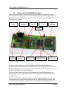
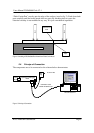
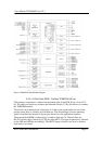
2.3. A Glance at the TOPAS900 Flash Board
After removing the plastic cover from the PCB you should see the following (for the
picture below the cable connection between the Programming-and Debugging Board and
the Flash Carrier Board has been removed to avoid covering components, this cable must
be plugged in by default):
RS232-Connector
D-SUB 9
Firmware-Processor
TMP87P808
Flash MCU
TMP95FY64F
Jumper for Carrier
Board Vcc
Programming Board <=>
Carrier Board Connectors
EA (external access)
Jumper
RESET and NMI
Switches
Power
Connector
Chip Select Jumpers
Status LED
Scratch on PCB
to break off
Figure 1 : The TOPAS900 Flash Board (Top View)
As shown in the picture above the TOPAS900 Flash PCB can be divided into two
functional groups: On the left side the “Programming- and Debugging- Board” is located.
On the right there is the “Flash Carrier Board”, surrounded by four 26-pin connectors (not
soldered). The PCB is delivered in one piece.
The Flash Carrier Board can also be used independently from the Programming and
Debugging Board. For independent usage it must be separated from the main board by
breaking it off.
To break the Flash Carrier Board off please use this technique: Remove the connection
cable between the two parts when plugged in. Put the TOPAS900 Flash board on a flat
and stable surface. Keep the scratch between “Programming-and-Debugging Part” and