


PCI v3.0.151 Getting Started Guide www.xilinx.com 31
UG157 August 31, 2005
Input Delay Buffers
R
IOBs of the FPGA device. The use of these delay buffers is selected through the
implementation specific constraints file
Some implementations use alternate delay buffers, selected via the CFG[248:245] bits in
the HDL configuration file. Table 3-3 shows the required settings for CFG[248:245] in
the HDL configuration file.
You must set CFG[248:245] appropriately for the selected implementation. While the
default setting is used for most implementations, failure to match the settings to the
selected implementation may result in hardware failures.
Virtex-4 implementations make use of the new IDELAY input delay buffer primitives. An
IDELAY input delay buffer is a calibrated and adjustable delay line. This delay mechanism
provides superior performance over the legacy input delay buffers. Be sure to observe the
settings shown in Table 3-3 and use the appropriate constraints file for the design.
Designs that use IDELAY primitives also require the use of the IDELAYCTRL primitive.
The function of the IDELAYCTRL primitive is to calibrate the IDELAY delay lines. To
perform this calibration, the IDELAYCTRL primitive requires a 200 MHz input clock. The
design and wrapper files for use with reference clocks contain IDELAY instances,
IDELAYCTRL instances, and an additional input, RCLK, for a 200 MHz reference clock
from an I/O pin. This reference clock is distributed to all applicable IDELAYCTRL
primitives using a global clock buffer.
It is important to note that there is some flexibility in the origin, generation, and use of this
200 MHz reference clock. The provided design and wrapper files represent a trivial case
that can may be modified to suit specific design requirements:
• For designs requiring IDELAY and IDELAYCTRL for other IP cores, or custom user
logic, the 200 MHz reference clock can be shared. It is possible to tap the reference
clock in the wrapper file, after it is driven by the global buffer. This signal may be
used by other IDELAY and IDELAYCTRL instances.
• For designs that already have a 200 MHz reference clock distributed on a global clock
buffer, this clock can be shared. The wrapper file can be modified to remove the
external I/O pin and the global clock buffer instance. Simply tap the existing 200 MHz
clock signal and bring it into the wrapper file for the interface to use.
• For designs that do not have a 200 MHz reference clock, it may be possible to generate
a 200 MHz reference clock using a Digital Clock Manager (DCM) and another clock.
The other clock may be available internally or externally, but must be fixed frequency.
In this case, it is the responsibility of the user to verify the following:
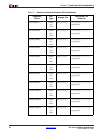
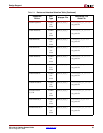
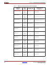
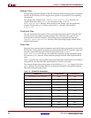
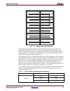
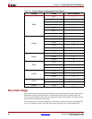
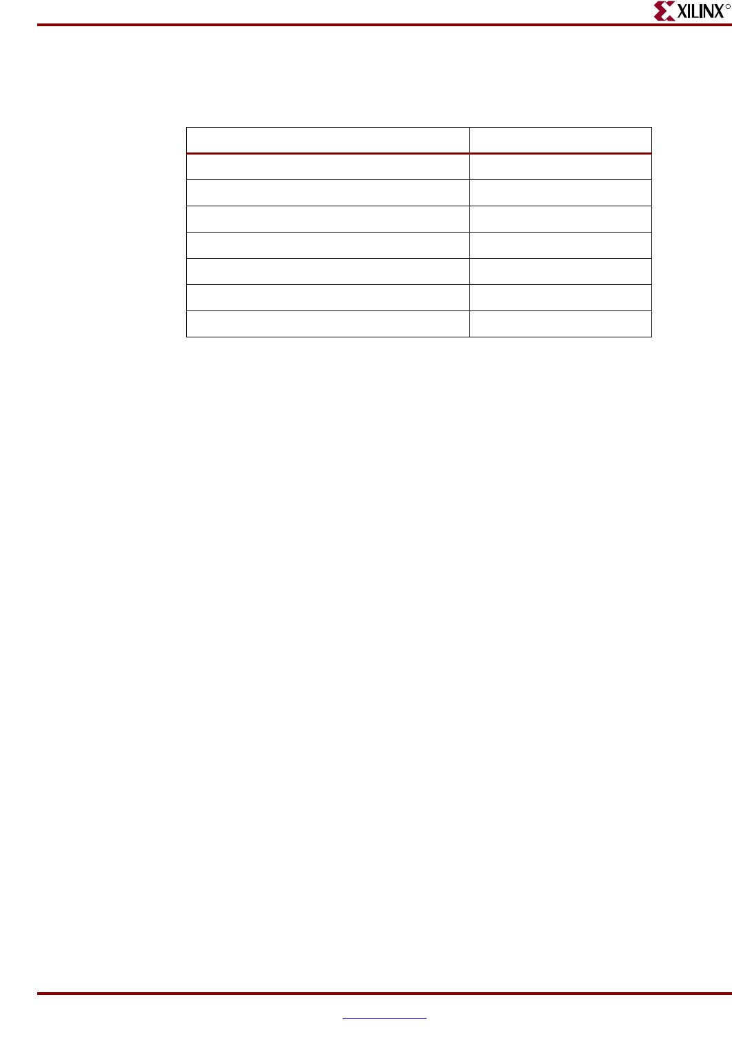
Table 3-3: Delay Buffer Settings
Implementation Delay Setting
Virtex, Virtex-E (All)
“0000”
Spartan-II, Spartan-IIE (All)
“0000”
Virtex-II, Spartan-3, Spartan-3E (All)
“0000”
Virtex-II Pro (All 33 MHz)
“0000”
Virtex-II Pro (All 66 MHz)
“0001”
Virtex-4 (Global Clock)
“0000”
Virtex-4 (Regional Clock)
“1000”