


32 www.xilinx.com PCI v3.0.151 Getting Started Guide
UG157 August 31, 2005
Chapter 3: Family Specific Considerations
R
1. The jitter of the source clock, to determine if it is appropriate for use as an input to
a DCM.
2. The DCM configuration, to generate a 200 MHz clock on any appropriate DCM
output (CLKFX, CLKDV, and so forth).
3. The jitter of the derived 200 MHz reference clock, to determine if it is appropriate
for use as an input to an IDELAYCTRL.
For more information about the relevant timing parameters, see the Virtex-4 Datasheet
and User Guide. As with the other implementation options, the derived 200 MHz
reference clock must be distributed by a global clock buffer to the IDELAYCTRL
instances.
Warning: The fixed frequency requirement of the source clock precludes the use of the PCI
bus clock, unless the design is used in an embedded/closed system where the PCI bus
clock is known to be a fixed frequency. See “Bus Clock Usage” for additional information
about the allowed behavior of the PCI bus clock in compliant systems.
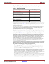
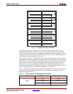
Regional Clock Usage
Some Virtex-4 implementations use a regional clock buffer (BUFR) for the PCI bus clock
instead of a global clock buffer (BUFG). Use of a regional clock resource greatly improves
the pin-to-pin clock to out of the interface while preserving full compliance. (Pin-to-pin
clock to out is a silicon (chip) performance parameter important for PCI.)
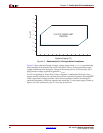
Designers must be aware of additional constraints imposed by the use of regional clocks.
Virtex-4 devices are divided into clock regions. Regional clock signals enter at the center of
a given region, and span the region of entry in addition to the region above and the region
below. The reach of a regional clock is physically limited to three clock regions. Figure 3-2
illustrates BUFR driving three clock regions. See the Virtex-4 Datasheet and User Guide for
more information about regional clocks.