


PCI v3.0.151 Getting Started Guide www.xilinx.com 33
UG157 August 31, 2005
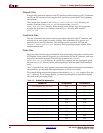
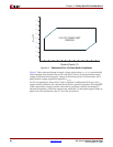
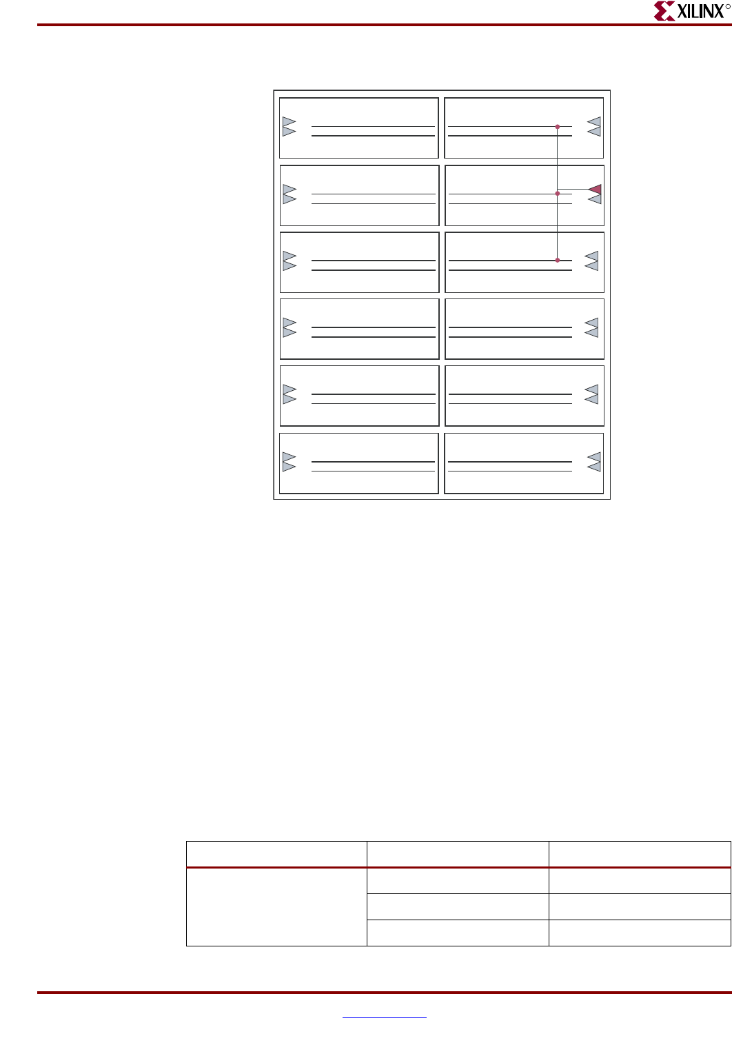
Regional Clock Usage
R
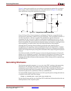
For designs using regional clocking, the PCI interface and those portions of the user
application clocked from the PCI bus clock must completely fit inside the three clock
regions accessible to the regional clock signal. This restriction limits the number of FPGA
resources that may be synchronous with the PCI bus clock. Access to additional logic is
available by crossing to another clock domain.
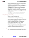
Clock regions are 16 CLB / 32 IOB tall and one-half the width of the device. With a regional
clock span limited to three regions, this yields a maximum of 96 IOB that may be used for
a PCI interface. A 64-bit PCI interface requires 90 IOB, and a 32-bit PCI interface requires 50
IOB. In some device and package combinations (typically, physically large devices in a
relatively low pin-count packages) not all IOB sites are bonded to package pins. This
renders some clock regions unusable for PCI purposes. This is generally not an issue for 32-
bit PCI interfaces; however, for 64-bit PCI interfaces, it is a concern.
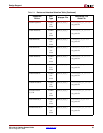
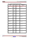
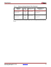
Table 3-4 defines all physically possible 64-bit PCI interfaces in various Virtex-4 device and
package combinations using regional clocks. Note that this does not apply to Virtex-4
designs using global clocks.
Figure 3-2: Regional Clocking Illustration
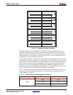
Table 3-4: Virtex-4 Device and Package 64-bit Interfaces
Package Device 64-bit Interfaces
SF363
LX15 none
LX25 none
FX12 none
BUFR