


PCI v3.0.151 Getting Started Guide www.xilinx.com 37
UG157 August 31, 2005
Generating Bitstreams
R
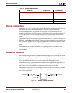
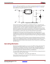
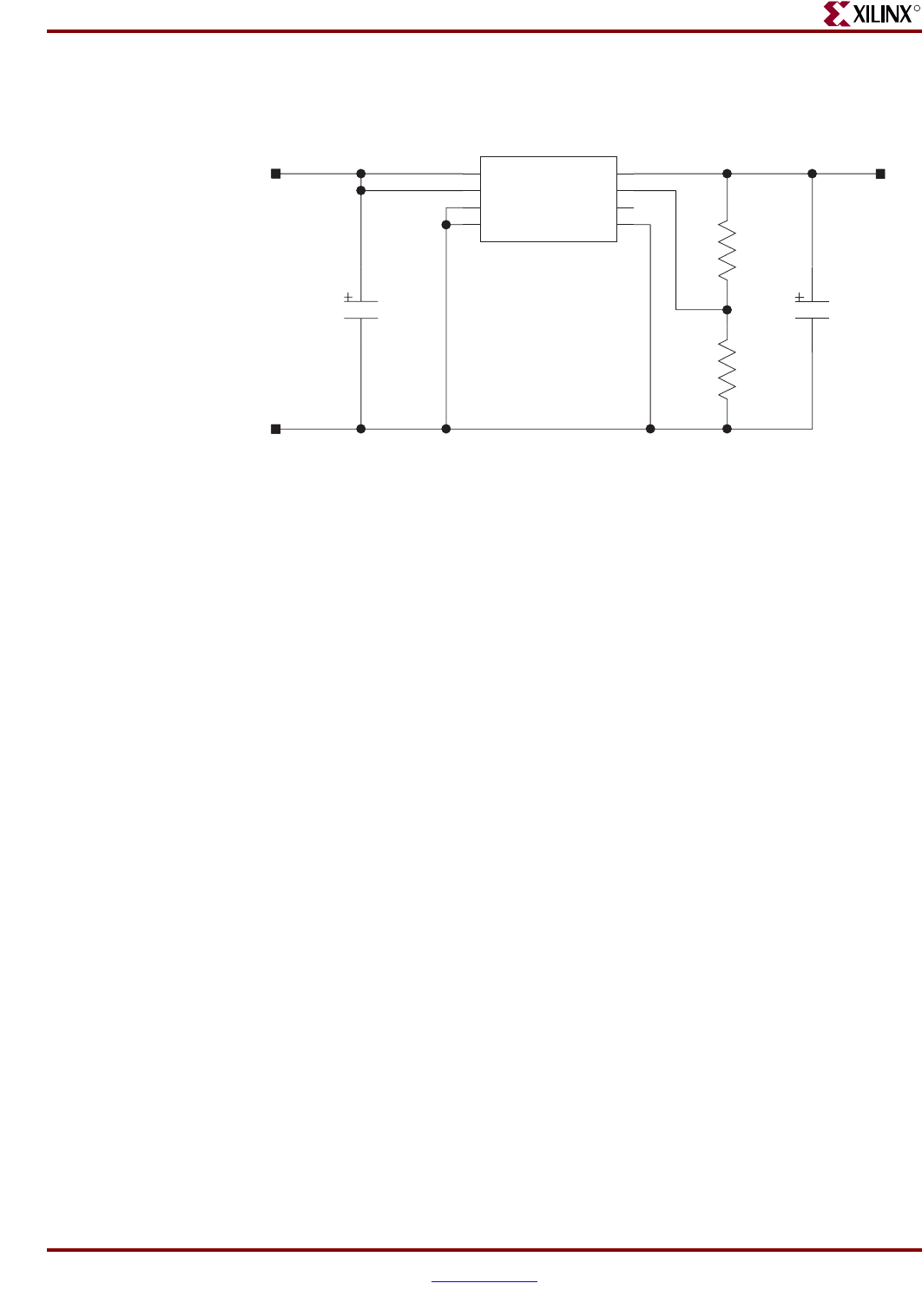
Figure 3-4 shows one possible low-cost solution to generate the required 3.0 volt output
driver supply. Xilinx recommends the use of the circuit shown in Figure 3-4, although
other approaches using other regulators are possible.
Virtex-II, Virtex-II Pro, Virtex-4, Spartan-3, and Spartan-3E devices, as specified in the
relevant device data sheets, exhibit a 10 pF pin capacitance. This is compliant with the PCI
Local Bus Specification, with one exception. The specification requires an 8 pF pin
capacitance for the IDSEL pin, to allow for non-resistive coupling to an AD[xx] pin. In
practice, this coupling may be resistive or non-resistive, and is performed on the system
board or backplane. For system board or backplane designs, use resistive coupling to avoid
non-compliance. For add-in cards, this is not under the control of the designer.
Although the PCI interface does not directly provide the PME# signal for power
management event reporting, it may be implemented by the user application. A typical
implementation would involve the implementation of the power management capability
item in user configuration space, along with a dedicated PME# output on a general purpose
I/O pin.
On all device families, if the FPGA power is removed, the general purpose I/O pin will
appear as a low impedance to ground. This appears to the system as an assertion of PME#.
For this reason, implementations that use the PME# signal should employ an external
buffering scheme that will prevent false assertions of PME# when power is removed from
the FPGA device.
Generating Bitstreams
The bitstream generation program, bitgen, may issue DRC warnings when generating
bitstreams for PCI designs. The number of these warnings varies depending on the
configuration options used for the PCI core. Typically, these warnings are related to nets
with no loads generated during trimming by the map program. Some of these nets are
intentionally preserved by statements in the user constraints file.
For some 66 MHz designs, bitgen must be run with a special option to change the behavior
of a global clock buffer used in the design:
bitgen -g Gclkdel<buf>:<opt> pcim_top_routed.ncd
See the release notes and the user constraints file for additional information about the use
and implications of this required option.
Figure 3-4: Output Driver VCCO Generation
GND
SUPPLY
+3.0V SUPPLY
26.1, 1%
1.0 uF
1
IN
GND
LT1763CS8
8
5
SHDN#
7
GND
6
OUT
ADJ
2
BYP
4
GND
33
4
2
6
7
5
3.3 uF
VCCO
38.3, 1%