36 www.xilinx.com SP605 Hardware User Guide
UG526 (v1.1.1) February 1, 2010
Chapter 1: SP605 Evaluation Board
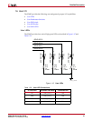
8-Kb NV Memory
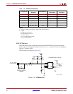
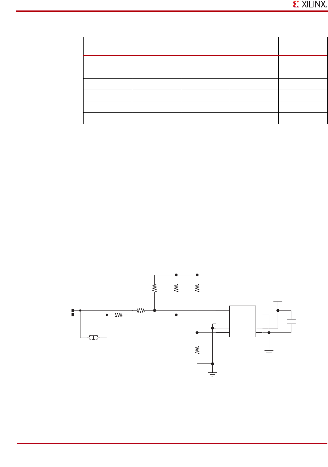
The SP605 hosts a 8-Kb ST Microelectronics M24C08-WDW6TP IIC parameter storage
memory device (U4). The IIC address of U4 is 0b1010100, and U4 is not write protected
(WP pin 7 is tied to GND).
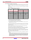
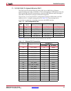
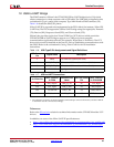
The IIC memory is shown in Figure 1-12.
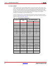
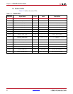
Table 1-19: IIC Bus Connections
U1 FPGA Pin
Schematic
Netname
Connected To
Level-Shifted
Connection
Level-Shifted
Net Name
R22 IIC_SDA_MAIN J2.C31, U4.5
(1)
– –
T21 IIC_SCL_MAIN J2.C30, U4.6
(1)
– –
AA4 IIC_SDA_DVI Q8.2, U31.14 Q8.3, P3.7 IIC_SDA_DVI_F
W13 IIC_SCL_DVI Q7.2, U31.15 Q7.3, P3.6 IIC_CLK_DVI_F
E6 IIC_SDA_SFP P2.4 – –
E5 IIC_SCL_SFP P2.5 – –
Notes:
1. U4 IIC bus signals are resistively coupled with 0 ohm resistors
2. Legend
J2, FMC LPC Connector
P2, SFP Module Connector
P3, DVI Connector
Qn.n, Level-Shifting Transistor
U31, Chrontel CH7301C
X-Ref Target - Figure 1-12
Figure 1-12: IIC Memory U4
VCC3V3
VCC3V3
SCL
SDA
A0
A1
A2
WP
VCC
GND
IIC Address 0b1010100
External Access
Header
1
2
R292
0
1/16W
5%
2
1
5%
1/16W
0
R291
2
1
5%
1/10W
1.0K
R6
IIC_SDA_MAIN
IIC_SCL_MAIN
12
H-1X2
J45
6
5
1
2
3
7
8
4
U4
M24C08-WDW6TP
2
1
C40
0.1UF
10V
X5R
1
2
R5
1.0K
1/10W
5%
1
2
R216
0
5%
1
2
1%
1/16W
DNP
R50
UG526_12 _100509


