MicroBlaze Development Kit Spartan-3E 1600 Edition User Guide 127
UG257 (v1.1) December 5, 2007 www.xilinx.com
R
Chapter 16
XC2C64A CoolRunner-II CPLD
The MicroBlaze Development Kit board includes a Xilinx XC2C64A CoolRunner-II CPLD.
The CPLD is user programmable and available for customer applications. Portions of the
CPLD are reserved to coordinate behavior between the various FPGA configuration
memories, namely the Xilinx Platform Flash PROM and the Intel StrataFlash PROM.
Consequently, the CPLD must provide the following functions in addition to the user
application.
x When the FPGA is in the Master Serial configuration mode (FPGA_M<2:0>=000),
generate an active-Low enable signal for the XCF04S Platform Flash PROM. The
Platform Flash PROM is disabled in all other configuration modes. The CPLD helps
reduce the number of jumpers on the board and simplifies the interaction of all the
possible FPGA configuration memory sources.
x When the FPGA is actively in the BPI-Up configuration mode (FPGA_M<2:0>=010,
DONE=0), set the upper five StrataFlash PROM address lines, A[24:20], to 00000
binary. When the FPGA is actively in the BPI-Down configuration mode
(FPGA_M<2:0>=011, DONE=0), set the upper five StrataFlash PROM address lines,
A[24:20], to 11111 binary. Set the upper five address lines to ZZZZZ for all non-BPI
configuration modes or whenever the FPGA’s DONE pin is High. This behavior is
identifical to the way the FPGA’s upper address lines function during BPI mode. So
why add a CPLD to mimic this behavior? A future reference design demonstrates
unique configuration capabilities. In a typical BPI-mode application, the CPLD is not
required.
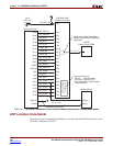
Other than the required CPLD functionality, there are between 13 to 21 user-I/O pins and
58 remaining macrocells available to the user application.
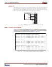
Jumper JP10 (WDT_EN) defines the state on the CPLD’s XC_WDT_EN signal. By default,
this jumper is empty and the signal is pulled to a logic High.
The XC_PROG_B output from the CPLD, if used, must be configured as an open-drain out
(i.e., either actively drives Low or floats to Hi-Z, never drives High). This signal connects
directly to the FPGA’s PROG_B programming pin.
The most-siginficant StrataFlash PROM address bit, SF_A<24>, is the same as the FX2
connector signal called FX2_IO<32>. The 16 Mbyte StrataFlash PROM only physically uses
the lower 24 bits, SF_A<23:0>. The extra address bit, SF_A<24>, is provided for upward
density migration for the StrataFlash PROM.


