MicroBlaze Development Kit Spartan-3E 1600 Edition User Guide 43
UG257 (v1.1) December 5, 2007 www.xilinx.com
Interaction with Intel StrataFlash
R
Interaction with Intel StrataFlash
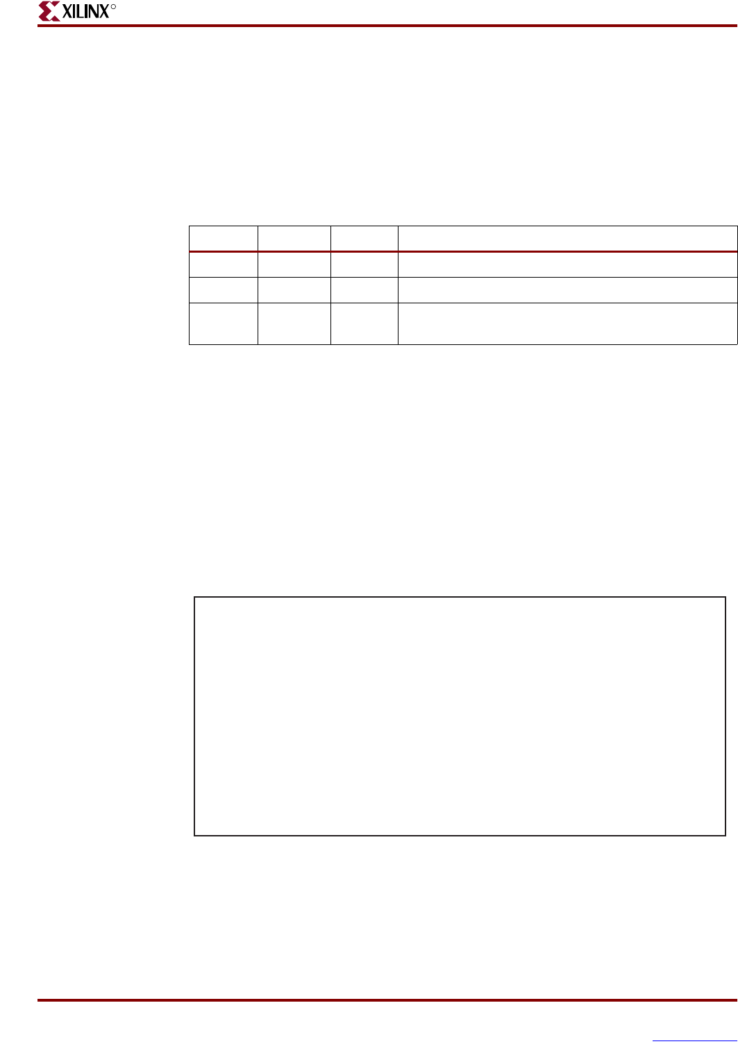
As shown in Figure 5-1, the four LCD data signals are also shared with StrataFlash data
lines SF_D<11:8>. As shown in Table 5-2, the LCD/StrataFlash interaction depends on the
application usage in the design. When the StrataFlash memory is disabled (SF_CE0 =
High), then the FPGA application has full read/write access to the LCD. Conversely, when
LCD read operations are disabled (LCD_RW = Low), then the FPGA application has full
read/write access to the StrataFlash memory
If the StrataFlash memory is in byte-wide (x8) mode (SF_BYTE = Low), the FPGA
application has full simultaneous read/write access to both the LCD and the StrataFlash
memory. In byte-wide mode, the StrataFlash memory does not use the SF_D<15:8> data
lines.
UCF Location Constraints
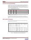
Figure 5-2 provides the UCF constraints for the Character LCD, including the I/O pin
assignment and the I/O standard used.
Table 5- 2: LCD/StrataFlash Control Interaction
SF_CE0 SF_BYTE LCD_RW Operation
1XXStrataFlash disabled. Full read/write access to LCD.
X X 0 LCD write access only. Full access to StrataFlash.
X0XStrataFlash in byte-wide (x8) mode. Upper address lines
are not used. Full access to both LCD and StrataFlash.
Notes:
1. ‘X’ indicates a don’t care, can be either 0 or 1.
Figure 5-2: UCF Location Constraints for the Character LCD
# ==== Character LCD (LCD) ====
NET "LCD_E" LOC = "M18" | IOSTANDARD = LVCMOS33 | DRIVE = 4 | SLEW = SLOW ;
NET "LCD_DI" LOC = "L18" | IOSTANDARD = LVCMOS33 | DRIVE = 4 | SLEW = SLOW ;
NET "LCD_RW" LOC = "L17" | IOSTANDARD = LVCMOS33 | DRIVE = 4 | SLEW = SLOW ;
NET "LCD_RET" LOC = "E3" | IOSTANDARD = SSTL2_I ;
NET "LCD_CS1" LOC = "P3" | IOSTANDARD = SSTL2_I ;
NET "LCD_CS2" LOC = "P4" | IOSTANDARD = SSTL2_I ;
# LCD data connections are shared with StrataFlash connections SF_D<15:8>
NET "SF_D<8>" LOC = "R15" | IOSTANDARD = LVCMOS33 | DRIVE = 4 | SLEW = SLOW ;
NET "SF_D<9>" LOC = "R16" | IOSTANDARD = LVCMOS33 | DRIVE = 4 | SLEW = SLOW ;
NET "SF_D<10>" LOC = "P17" | IOSTANDARD = LVCMOS33 | DRIVE = 4 | SLEW = SLOW ;
NET "SF_D<11>" LOC = "M15" | IOSTANDARD = LVCMOS33 | DRIVE = 4 | SLEW = SLOW ;
NET "SF_D<12>" LOC = "M16" | IOSTANDARD = LVCMOS33 | DRIVE = 4 | SLEW = SLOW ;
NET "SF_D<13>" LOC = "P6" | IOSTANDARD = LVCMOS33 | DRIVE = 4 | SLEW = SLOW ;
NET "SF_D<14>" LOC = "R8" | IOSTANDARD = LVCMOS33 | DRIVE = 4 | SLEW = SLOW ;
NET "SF_D<15>" LOC = "T8" | IOSTANDARD = LVCMOS33 | DRIVE = 4 | SLEW = SLOW ;
UG257_05_02_061306


