


REV. B
ADuC812
–10–
OVERVIEW OF MCU-RELATED SFRs
Accumulator SFR
ACC is the Accumulator register and is used for math opera-
tions including addition, subtraction, integer multiplication and
division, and Boolean bit manipulations. The mnemonics for
accumulator-specific instructions refer to the Accumulator as A.
B SFR
The B register is used with the ACC for multiplication and
division operations. For other instructions it can be treated as a
general-purpose scratchpad register.
Stack Pointer SFR
The SP register is the stack pointer and is used to hold an inter-
nal RAM address that is called the “top of the stack.” The SP
register is incremented before data is stored during PUSH and
CALL executions. While the Stack may reside anywhere in
on-chip RAM, the SP register is initialized to 07H after a reset.
This causes the stack to begin at location 08H.
Data Pointer
The Data Pointer is made up of three 8-bit registers, named
DPP (page byte), DPH (high byte) and DPL (low byte). These
are used to provide memory addresses for internal and external
code access and external data access. It may be manipulated as a
16-bit register (DPTR = DPH, DPL), although INC DPTR
instructions will automatically carry over to DPP, or as three
independent 8-bit registers (DPP, DPH, DPL).
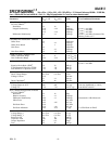
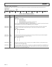
Program Status Word SFR
The PSW register is the Program Status Word which contains
several bits reflecting the current status of the CPU as detailed
in Table I.
SFR Address D0H
Power ON Default Value 00H
Bit Addressable Yes
YCCA0F1SR0SRVO1FP
Table I. PSW SFR Bit Designations
Bit Name Description
7 CY Carry Flag
6 AC Auxiliary Carry Flag
5 F0 General-Purpose Flag
4 RS1 Register Bank Select Bits
3 RS0 RS1 RS0 Selected Bank
000
011
102
113
2 OV Overflow Flag
1 F1 General-Purpose Flag
0 P Parity Bit
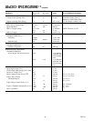
Power Control SFR
The Power Control (PCON) register contains bits for power-
saving options and general-purpose status flags as shown in
Table II.
SFR Address 87H
Power ON Default Value 00H
Bit Addressable No
DOMSDPIRESDPOTNIFFOELA1FG0FGDPLDI
Table II. PCON SFR Bit Designations
Bit Name Description
7 SMOD Double UART Baud Rate
6 ——— Reserved
5 ——— Reserved
4 ALEOFF Disable ALE Output
3 GF1 General-Purpose Flag Bit
2 GF0 General-Purpose Flag Bit
1 PD Power-Down Mode Enable
0 IDL Idle Mode Enable