


REV. B
ADuC812
–29–
8051-COMPATIBLE ON-CHIP PERIPHERALS
This section gives a brief overview of the various secondary
peripheral circuits that are also available to the user on-chip.
These remaining functions are fully 8051-compatible and are
controlled via standard 8051 SFR bit definitions.
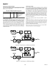
Parallel I/O Ports 0–3
The ADuC812 uses four input/output ports to exchange data with
external devices. In addition to performing general-purpose I/O,
some ports are capable of external memory operations; others are
multiplexed with an alternate function for the peripheral features
on the device. In general, when a peripheral is enabled, that pin
may not be used as a general purpose I/O pin.
Port 0 is an 8-bit open drain bidirectional I/O port that is directly
controlled via the P0 SFR (SFR address = 80 hex). Port 0 pins
that have 1s written to them via the Port 0 SFR will be configured
as open drain and will therefore float. In that state, Port 0 pins
can be used as high impedance inputs. An external pull-up
resistor will be required on Port 0 outputs to force a valid logic
high level externally. Port 0 is also the multiplexed low-order
address and data bus during accesses to external program or data
memory. In this application it uses strong internal pull-ups when
emitting 1s.
Port 1 is also an 8-bit port directly controlled via the P1 SFR
(SFR address = 90 hex). Port 1 ia an input only port. Port 1
digital output capability is not supported on this device. Port 1
pins can be configured as digital inputs or analog inputs.
By (power-on) default these pins are configured as Analog Inputs,
i.e., “1” written in the corresponding Port 1 register bit. To
configure any of these pins as digital inputs, the user should
write a “0” to these port bits to configure the corresponding pin
as a high impedance digital input.
These pins also have various secondary functions described in
Table XIV.
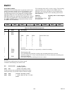
Table XIV. Port 1, Alternate Pin Functions
Pin Alternate Function
P1.0 T2 (Timer/Counter 2 External Input)
P1.1 T2EX (Timer/Counter 2 Capture/Reload Trigger)
P1.5 SS (Slave Select for the SPI interface)
Port 2 is a bidirectional port with internal pull-up resistors directly
controlled via the P2 SFR (SFR address = A0 hex). Port 2 pins
that have 1s written to them are pulled high by the internal pull-up
resistors and, in that state, they can be used as inputs. As inputs,
Port 2 pins being pulled externally low will source current because
of the internal pull-up resistors. Port 2 emits the high order
address bytes during fetches from external program memory
and middle and high order address bytes during accesses to the
24-bit external data memory space.
Port 3 is a bidirectional port with internal pull-ups directly
controlled via the P3 SFR (SFR address = B0 hex). Port 3 pins
that have 1s written to them are pulled high by the internal pull-
ups and in that state they can be used as inputs. As inputs, Port
3 pins being pulled externally low will source current because of
the internal pull-ups. Port 3 pins also have various secondary
functions described in Table XV.
Table XV. Port 3, Alternate Pin Functions
Pin Alternate Function
P3.0 RXD (UART Input Pin)
(or Serial Data I/O in Mode 0)
P3.1 TXD (UART Output Pin)
(or Serial Clock Output in Mode 0)
P3.2 INT0 (External Interrupt 0)
P3.3 INT1 (External Interrupt 1)
P3.4 T0 (Timer/Counter 0 External Input)
P3.5 T1 (Timer/Counter 1 External Input)
P3.6 WR (External Data Memory Write Strobe)
P3.7 RD (External Data Memory Read Strobe)
The alternate functions of P1.0, P1.1, P1.5 and Port 3 pins can
only be activated if the corresponding bit latch in the P1 and
P3 SFRs contains a 1. Otherwise, the port pin is stuck at 0.
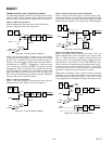
Timers/Counters
The ADuC812 has three 16-bit Timer/Counters: Timer 0,
Timer 1, and Timer 2. The Timer/Counter hardware has been
included on-chip to relieve the processor core of the overhead
inherent in implementing timer/counter functionality in soft-
ware. Each Timer/Counter consists of two 8-bit registers THx and
TLx (x = 0, 1 and 2). All three can be configured to operate
either as timers or event counters.
In “Timer” function, the TLx register is incremented every
machine cycle. Thus one can think of it as counting machine
cycles. Since a machine cycle consists of 12 core clock periods,
the maximum count rate is 1/12 of the core clock frequency.
In “Counter” function, the TLx register is incremented by a 1-to-0
transition at its corresponding external input pin, T0, T1, or T2.
In this function, the external input is sampled during S5P2 of
every machine cycle. When the samples show a high in one cycle
and a low in the next cycle, the count is incremented. The new
count value appears in the register during S3P1 of the cycle follow-
ing the one in which the transition was detected. Since it takes two
machine cycles (24 core clock periods) to recognize a 1-to-0 transi-
tion, the maximum count rate is 1/24 of the core clock frequency.
There are no restrictions on the duty cycle of the external
input signal, but to ensure that a given level is sampled at
least once before it changes, it must be held for a minimum of
one full machine cycle.