


REV. B
ADuC812
–39–
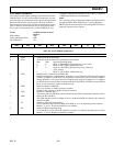
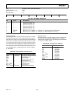
IE2: Secondary Interrupt Enable Register
SFR Address A9H
Power-On Default Value 00H
Bit Addressable No
—————— IMSPEISE
Table XXV. IE2 SFR Bit Designations
Bit Name Description
7 — Reserved for Future Use.
6 — Reserved for Future Use.
5 — Reserved for Future Use.
4 — Reserved for Future Use.
3 — Reserved for Future Use.
2 — Reserved for Future Use.
1 EPSMI Written by User to Enable “1” or Disable “0” Power Supply Monitor Interrupt.
0 ESI Written by User to Enable “1” or Disable “0” SPI/I
2
C Serial Port Interrupt.
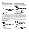
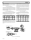
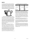
Interrupt Priority
The Interrupt Enable registers are written by the user to enable
individual interrupt sources, while the Interrupt Priority registers
allow the user to select one of two priority levels for each interrupt.
An interrupt of a high priority may interrupt the service routine
of a low priority interrupt, and if two interrupts of different priority
occur at the same time, the higher level interrupt will be serviced
first. An interrupt cannot be interrupted by another interrupt of
the same priority level. If two interrupts of the same priority level
occur simultaneously, a polling sequence is observed as shown
in Table XXVI.
Table XXVI. Priority within an Interrupt Level
Source Priority Description
PSMI 1 (Highest) Power Supply Monitor Interrupt
IE0 2 External Interrupt 0
ADCI 3 ADC Interrupt
TF0 4 Timer/Counter 0 Interrupt
IE1 5 External Interrupt 1
TF1 6 Timer/Counter 1 Interrupt
I2CI + ISPI 7 I
2
C/SPI Interrupt
RI + TI 8 Serial Interrupt
TF2 + EXF2 9 (Lowest) Timer/Counter 2 Interrupt
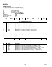
Interrupt Vectors
When an interrupt occurs the program counter is pushed onto
the stack and the corresponding interrupt vector address is
loaded into the program counter. The interrupt Vector Addresses
are shown in the Table XXVII.
Table XXVII. Interrupt Vector Addresses
Source Vector Address
IE0 0003 Hex
TF0 000B Hex
IE1 0013 Hex
TF1 001B Hex
RI + TI 0023 Hex
TF2 + EXF2 002B Hex
ADCI 0033 Hex
I2CI + ISPI 003B Hex
PSMI 0043 Hex