


REV. B
ADuC812
–19–
Using the Flash/EE Program Memory
This 8K Byte Flash/EE Program Memory array is mapped
into the lower 8K bytes of the 64K bytes program space addres-
sable by the ADuC812 and will be used to hold user code in
typical applications.
The program memory array can be programmed in one of two
modes, namely:
Serial Downloading (In-Circuit Programming)
As part of its embedded download/debug kernel, the ADuC812
facilitates serial code download via the standard UART serial port.
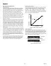
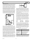
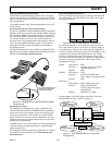
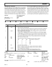
Serial download mode is automatically entered on power-up if
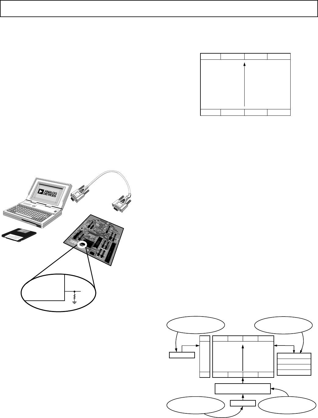
the external pin, PSEN, is pulled low through an external resis-
tor as shown in Figure 15. Once in this mode, the user can
download code to the program memory array while the device is
sited in its target application hardware. A PC serial download
executable is provided as part of the ADuC812 QuickStart
development system.
The Serial Download protocol is detailed in a MicroConverter
Applications Note uC004 available from the ADI MicroConverter
Website at www.analog.com/micronverter.
1k⍀
PSEN
ADuC812
PULL PSEN LOW DURING RESET TO
CONFIGURE THE ADuC812 FOR
SERIAL DOWNLOAD MODE
Figure 15. Flash/EE Memory Serial Download Mode
Programming
Parallel Programming
The parallel programming mode is fully compatible with
conventional third party Flash or EEPROM device programmers.
In this mode Ports P0, P1 and P2 operate as the external data
and address bus interface, ALE operates as the Write Enable
strobe and Port P3 is used as a general configuration port that
configures the device for various program and erase operations
during parallel programming.
The high voltage (12 V) supply required for Flash programming
is generated using on-chip charge pumps to supply the high
voltage program lines.
The complete parallel programming specification is available
on the MicroConverter home page at www.analog.com/
microconverter.
U
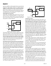
sing the Flash/EE Data Memory
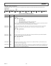
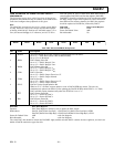
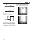
The user Flash/EE data memory array consists of 640 bytes that
are configured into 160 (Page 00H to Page 9FH), 4-byte pages
as shown in Figure 16.
9FH
BYTE 1 BYTE 2 BYTE 3 BYTE 4
00H
BYTE 1 BYTE 2 BYTE 3 BYTE 4
Figure 16. User Flash/EE Memory Configuration
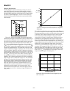
As with other ADuC812 user-peripherals circuits, the inter-
face to this memory space is via a group of registers mapped
in the SFR space. A group of four data registers (EDATA1-4)
are used to hold the 4-byte page being accessed. EADRL is used
to hold the 8-bit address of the page being accessed. Finally,
ECON is an 8-bit control register that may be written with
one of five Flash/EE memory access commands to trigger various
read, write, erase and verify functions. These register can be
summarized as follows:
ECON: SFR Address: B9H
Function: Controls access to 640 Bytes
Flash/EE Data Space.
Default: 00H
EADRL: SFR Address: C6H
Function: Holds the Flash/EE Data
Page Address. 0 through 9F Hex
Default: 00H
EDATA 1–4:
SFR Address: BCH to BFH respectively
Function: Holds Flash/EE Data
memory page write or page
read data bytes.
Default : EDATA1–4 –> 00H
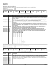
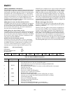
A block diagram of the SFR registered interface to the Data
Flash/EE Memory array is shown in Figure 17.
9FH
BYTE 1
BYTE 2
BYTE 3
BYTE 4
00H
EDATA1 (BYTE 1)
EDATA2 (BYTE 2)
EDATA3 (BYTE 3)
EDATA4 (BYTE 4)
EADRL
ECON COMMAND
INTERPRETER LOGIC
ECON
BYTE 1 BYTE 2 BYTE 3 BYTE 4
FUNCTION:
HOLDS THE 8-BIT PAGE
ADDRESS POINTER
FUNCTION:
HOLDS COMMAND WORD
FUNCTION:
HOLDS THE 4-BYTE
PAGE WORD
FUNCTION:
INTERPRETS THE FLASH
COMMAND WORD
Figure 17. User Flash/EE Memory Control and
Configuration