


REV. B
ADuC812
–16–
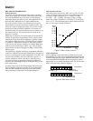
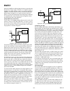
ground, no amplifier can deliver signals all the way to ground when
powered by a single supply. Therefore, if a negative supply is
available, you might consider using it to power the front-end
amplifiers. If you do, however, be sure to include the Schottky
diodes shown in Figure 8 (or at least the lower of the two
diodes) to protect the analog input from undervoltage conditions.
To summarize this section, use the circuit of Figure 8 to drive
the analog input pins of the ADuC812.
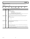
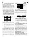
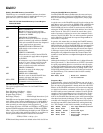
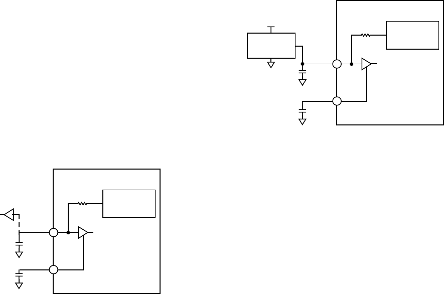
Voltage Reference Connections
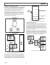
The on-chip 2.5 V bandgap voltage reference can be used as the
reference source for the ADC and DACs. In order to ensure
the accuracy of the voltage reference you must decouple both
the V
REF
pin and the C
REF
pin to ground with 0.1 µF ceramic
chip capacitors as shown in Figure 9.
8
0.1F
BUFFER
V
REF
0.1F
C
REF
7
BUFFER
51⍀
2.5V
BANDGAP
REFERENCE
ADuC812
Figure 9. Decoupling V
REF
and C
REF
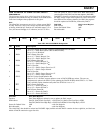
The internal voltage reference can also be tapped directly from
the V
REF
pin, if desired, to drive external circuitry. However, a
buffer must be used in this case to ensure that no current is
drawn from the V
REF
pin itself. The voltage on the C
REF
pin is
that of an internal node within the buffer block, and its voltage
is critical to ADC and DAC accuracy. Do not connect anything
to this pin except the capacitor, and be sure to keep trace-
lengths short on the C
REF
capacitor, decoupling the node
straight to the underlying ground plane.
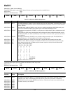
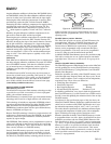
The ADuC812 powers up with its internal voltage reference in
the “off” state. The voltage reference turns on automatically
whenever the ADC or either DAC gets enabled in software.
Once enabled, the voltage reference requires approximately
65 ms to power up and settle to its specified value. Be sure that
your software allows this time to elapse before initiating any
conversions. If an external voltage reference is preferred, simply
connect it to the V
REF
pin as shown in Figure 10 to overdrive
the internal reference.
To ensure accurate ADC operation, the voltage applied to V
REF
must be between 2.3 V and AV
DD
. In situations where analog
input signals are proportional to the power supply (such as some
strain-gage applications) it can be desirable to connect the V
REF
pin directly to AV
DD
. In such a configuration you must also
connect the C
REF
pin directly to AV
DD
to circumvent internal
buffer headroom limitations. This allows the ADC input trans-
fer function to accurately span the full range 0 to AV
DD
.
Operation of the ADC or DACs with a reference voltage below
2.3 V, however, may incur loss of accuracy eventually resulting
in missing codes or nonmonotonicity. For that reason, do not
use a reference voltage less than 2.3 V.
8
0.1F
V
REF
0.1F
C
REF
7
BUFFER
51⍀
2.5V
BANDGAP
REFERENCE
ADuC812
EXTERNAL
VOLTAGE
REFERENCE
V
DD
Figure 10. Using an External Voltage Reference
Configuring the ADC
The three SFRs (ADCCON1, ADCCON2, ADCCON3) con-
figure the ADC. In nearly all cases, an acquisition time of 1 ADC
clock (ADCCON1.2 = 0, ADCCON1.3 = 0) will provide plenty
of time for the ADuC812 to acquire its signal before switching
the internal track and hold amplifier in to hold mode. The
only exception would be a high source impedance analog
input, but these should be buffered first anyway since source
impedances of greater than 610 Ω can cause dc errors as well.
The ADuC812’s successive approximation ADC is driven by a
divided down version of the master clock. To ensure adequate
ADC operation, this ADC clock must be between 400 kHz and
4 MHz, and optimum performance is obtained with ADC clock
between 400 kHz and 3 MHz. Frequencies within this range can
easily be achieved with master clock frequencies from 400 kHz to
well above 16 MHz with the four ADC clock divide ratios to
choose from. For example, with a 12 MHz master clock, set the
ADC clock divide ratio to 4 (i.e., ADCCLK = MCLK/4 = 3 MHz)
by setting the appropriate bits in ADCCON1 (ADCCON1.5 = 1,
ADCCON1.4 = 0).
The total ADC conversion time is 15 ADC clocks, plus 1 ADC
clock for synchronization, plus the selected acquisition time (1,
2, 3, or 4 ADC clocks). For the example above, with a 1 clock
acquisition time, total conversion time is 17 ADC clocks (or
5.67 µs for a 3 MHz ADC clock).
In continuous conversion mode, a new conversion begins each
time the previous one finishes. The sample rate is then simply
the inverse of the total conversion time described above. In the
example above, the continuous conversion mode sample rate
would be 176.5 kHz.
ADC DMA Mode
The on-chip ADC has been designed to run at a maximum
conversion speed of 5 µs (200 kHz sampling rate). When con-
verting at this rate the ADuC812 micro has 5 µs to read the
ADC result and store the result in memory for further post
processing all within 5 µs otherwise the next ADC sample could
be lost. In an interrupt driven routine the micro would also have
to jump to the ADC Interrupt Service routine which will also
increase the time required to store the ADC results. In applica-
tions where the ADuC812 cannot sustain the interrupt rate, an
ADC DMA mode is provided.
To enable DMA mode, Bit 6 in ADCCON2 (DMA) must be
set. This allows the ADC results to be written directly to a
16 MByte external static memory SRAM (mapped into data
memory space) without any interaction from the ADuC812