


REV. B
ADuC812
–23–
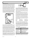
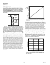
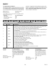
SOURCE/SINK CURRENT – mA
3
0 5 10 15
OUTPUT VOLTAGE – V
2
1
0
Figure 21. Source and Sink Current Capability with
V
REF
= V
DD
= 3 V
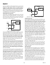
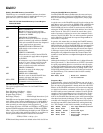
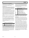
To drive significant loads with the DAC outputs, external buff-
ering may be required, as illustrated in Figure 22.
9
ADuC812
10
Figure 22. Buffering the DAC Outputs
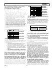
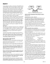
The DAC output buffer also features a high-impedance disable
function. In the chip’s default power-on state, both DACs are
disabled, and their outputs are in a high-impedance state (or
“three-state”) where they remain inactive until enabled in software.
This means that if a zero output is desired during power-up or
power-down transient conditions, then a pull-down resistor must
be added to each DAC output. Assuming this resistor is in place,
the DAC outputs will remain at ground potential whenever the
DAC is disabled. However, each DAC output will still spike
briefly when you first apply power to the chip, and again when
each DAC is first enabled in software. Typical scope shots of
these spikes are given in Figure 23 and Figure 24 respectively.
200
s/DIV
AV
DD
– 2V/DIV
DAC OUT – 500mv/DIV
Figure 23. DAC Output Spike at Chip Power-Up
5
s/DIV, 1V/DIV
Figure 24. DAC Output Spike at DAC Enable