


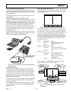
REV. B
ADuC812
–15–
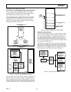
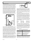
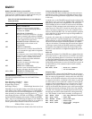
Driving the A/D Converter
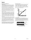
The ADC incorporates a successive approximation (SAR) archi-
tecture involving a charge-sampled input stage. Figure 7 shows
the equivalent circuit of the analog input section. Each ADC
conversion is divided into two distinct phases as defined by the
position of the switches in Figure 7. During the sampling phase
(with SW1 and SW2 in the “track” position) a charge propor-
tional to the voltage on the analog input is developed across the
input sampling capacitor. During the conversion phase (with
both switches in the “hold” position) the capacitor DAC is
adjusted via internal SAR logic until the voltage on node A is
zero indicating that the sampled charge on the input capacitor is
balanced out by the charge being output by the capacitor DAC.
The digital value finally contained in the SAR is then latched
out as the result of the ADC conversion. Control of the SAR,
and timing of acquisition and sampling modes, is handled
automatically by built-in ADC control logic. Acquisition and
conversion times are also fully configurable under user control.
ADuC812
TEMPERATURE
SENSOR
AIN0
AIN7
200⍀
SW1
2pF
NODE A
COMPARATOR
SW2
HOLDTRACK
AGND
TRACK
HOLD
CAPACITOR
DAC
Figure 7. Internal ADC Structure
Note that whenever a new input channel is selected, a residual
charge from the 2 pF sampling capacitor places a transient on
the newly selected input. The signal source must be capable of
recovering from this transient before the sampling switches click
into “hold” mode. Delays can be inserted in software (between
channel selection and conversion request) to account for input
stage settling, but a hardware solution will alleviate this burden
from the software design task and will ultimately result in a
cleaner system implementation. One hardware solution would
be to choose a very fast settling op amp to drive each analog
input. Such an op amp would need to fully settle from a small
signal transient in less than 300 ns in order to guarantee adequate
settling under all software configurations. A better solution, recom-
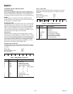
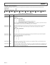
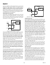
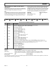
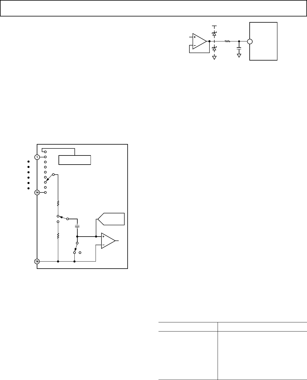
mended for use with any amplifier, is shown in Figure 8.
Though at first glance the circuit in Figure 8 may look like a
simple antialiasing filter, it actually serves no such purpose since
its corner frequency is well above the Nyquist frequency, even at
a 200 kHz sample rate. Though the R/C does helps to reject some
incoming high-frequency noise, its primary function is to ensure
that the transient demands of the ADC input stage are met. It
ADuC812
AIN0
1
0.01F
51⍀
Figure 8. Buffering Analog Inputs
does so by providing a capacitive bank from which the 2 pF sam-
pling capacitor can draw its charge. Since the 0.01 µF capacitor
in Figure 8 is more than 4096 times the size of the 2 pF sam-
pling capacitor, its voltage will not change by more than one
count (1/4096) of the 12-bit transfer function when the 2 pF
charge from a previous channel is dumped onto it. A larger
capacitor can be used if desired, but not a larger resistor (for
reasons described below).
The Schottky diodes in Figure 8 may be necessary to limit the
voltage applied to the analog input pin as per the data sheet
absolute maximum ratings. They are not necessary if the op
amp is powered from the same supply as the ADuC812 since
in that case the op amp is unable to generate voltages above
V
DD
or below ground. An op amp of some kind is necessary
unless the signal source is very low impedance to begin with.
DC leakage currents at the ADuC812’s analog inputs can
cause measurable dc errors with external source impedances
as little as 100 Ω or so. To ensure accurate ADC operation, keep
the total source impedance at each analog input less than 61 Ω.
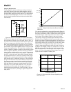
The table below illustrates examples of how source impedance
can affect dc accuracy.
Source Error from 1 µA Error from 10 µA
Impedance Leakage Current Leakage Current
61 Ω 61 µV = 0.1 LSB 610 µV = 1 LSB
610 Ω 610 µV = 1 LSB 6.1 mV = 10 LSB
Although Figure 8 shows the op amp operating at a gain of 1,
you can of course configure it for any gain needed. Also, you
can just as easily use an instrumentation amplifier in its place to
condition differential signals. Use any modern amplifier that is
capable of delivering the signal (0 to V
REF
) with minimal satura-
tion. Some single-supply rail-to-rail op amps that are useful for
this purpose include, but are certainly not limited to, the ones
given in Table VI. Check Analog Devices literature (CD ROM
data book, etc.) for details on these and other op amps and
instrumentation amps.
Table VI. Some Single-Supply Op Amps
Op Amp Model Characteristics
OP181/OP281/OP481 Micropower
OP191/OP291/OP491 I/O Good up to V
DD
, Low Cost
OP196/OP296/OP496 I/O to V
DD
, Micropower, Low Cost
OP183/OP283 High Gain-Bandwidth Product
OP162/OP262/OP462 High GBP, Micro Package
AD820/AD822/AD824 FET Input, Low Cost
AD823 FET Input, High GBP
Keep in mind that the ADC’s transfer function is 0 to V
REF
, and
any signal range lost to amplifier saturation near ground will
impact dynamic range. Though the op amps in Table VI are
capable of delivering output signals very closely approaching