


REV. B
ADuC812
–25–
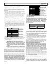
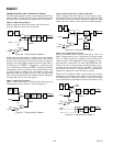
POWER SUPPLY MONITOR
As its name suggests, the Power Supply Monitor, once enabled,
monitors both supplies (AV
DD
and DV
DD
) on the ADuC812. It
will indicate when either power supply drops below one of five
user-selectable voltage trip points from 2.63 V to 4.63 V. For
correct operation of the Power Supply Monitor function, AV
DD
must be equal to or greater than 2.7 V. The Power Supply
Monitor function is controlled via the PSMCON SFR. If
enabled via the IE2 SFR, the Power Supply Monitor will interrupt
the core using the PSMI bit in the PSMCON SFR. This bit will
not be cleared until the failing power supply has returned
above the trip point for at least 256 ms. This is to ensure that
the power supply has fully settled before the bit is cleared. This
monitor function allows the user to save working registers to avoid
possible data loss due to the low supply condition, and also ensures
that normal code execution will not resume until a safe supply
level has been well established. The supply monitor is also
protected against spurious glitches triggering the interrupt circuit.
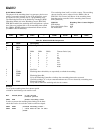
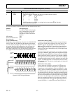
PSMCON Power Supply Monitor
Control Register
SFR Address DFH
Power-On Default Value DCH
Bit Addressable No
Table X. PSMCON SFR Bit Designations
Bit Name Description
7 — Not Used.
6 CMP AV
DD
and DV
DD
Comparator Bit.
This is a read-only bit and directly reflects the state of the AV
DD
and DV
DD
comparators.
Read “1” indicates that both AV
DD
and DV
DD
supply are above its selected trip point.
Read “0” indicates that either AV
DD
or DV
DD
supply are below its selected trip point.
5 PSMI Power Supply Monitor Interrupt Bit.
This bit will be set high by the MicroConverter if CMP is low, indicating low analog
or digital supply. The PSMI bit can be used to interrupt the processor. Once CMPD
and/or CMP return (and remain) high, a 256 ms counter is started. When this counter
times out, the PSMI interrupt is cleared. PSMI can also be written by the user. How
ever, if either comparator output is low, it is not possible for the user to clear PSMI.
4 TP2 VDD Trip Point Selection Bits.
3 TP1
2 TP0 These bits select the AV
DD
and DVDD trip-point voltage as follows:
TP2 TP1 TP0 Selected DV
DD
Trip Point (V)
0004.63
0014.37
0103.08
0112.93
1002.63
1 PSF
AV
DD
/
DV
DD
fault indicator
Read “1” indicates that the AV
DD
supply caused the fault condition.
Read “0” indicates that the DV
DD
supply caused the fault condition.
0 PSMEN Power Supply Monitor Enable Bit.
Set to
“1”
by the user to enable the Power Supply Monitor Circuit.
Cleared to “0” by the user to disable the Power Supply Monitor Circuit.
Example
To configure the PSM for a trippoint of 4.37 V, the following
code would be used
MOV PSMCON,#005h ;enable PSM with
;4.37V threshold
SETB EA ;enable interrupts
MOV IE2,#002h ;enable PSM
;interrupt
If the supply voltage falls below this level, the PC would vector
to the ISR.
ORG 0043h ;PSM ISR
CHECK:MOV A,PSMCON ;PSMCON.5 is the
;PSM interrupt
;bit..
JB ACC.5,CHECK ;..it is cleared
;only when Vdd
;has remained
;above the trip
;point for 256ms
;or more.
RETI ; return only when "all's well"
—PMCIMSP2PT1PT0PTFSPNEMSP