


Service Manual
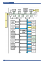
System Outline
4-6
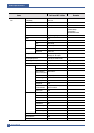
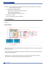
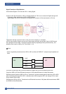
4.1.4 Scan Part
Pictorial signal input part: output signal of CCD passes through Bypass Cap change to ADC at HT82V26, and
defined signal between HT82V26 and CHORUSm processes the Image signal. When AFE accept each pixel,
CDS(Correlated Double Sampling ) technique which samples arm-level twice is used on each pixel by using
CIP4e signal.
2) Pictorial image processing part: read CCD Pixel data in terms of 600dpi Line and process Error Diffusion
Algorithm on Text mode and Photo mode, and then store Data at Scan Buf fer on PC Scan mode without algo-
rithm.
On every mode Shading Correction and Gamma Correction are executed ahead, then processing is executed
later.
* Scan Image Control Specification
Minimum Scan Line Time: 0.75ms
Scan Resolution : Max. 600DPI
Scan Width : 216mm
main function
- Internal 12bit ADC
- White Shading Correction
- Gamma Correction
- CCD Interface
- 256 Gray Scale
3) CCD Operating Part : CCD Image sensor use +5V and Inverter uses +24V
- CCD Maximum Operating Frequency : 10MHz
- CCD Line time : 0.75ms
- White Data output Voltage : 0.7V 0.5V (Mono Copy, 0.75ms/line)
- Maximum Inverter Current : 600 mA Max.( +24V)
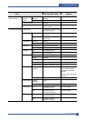
4.1.5 OPE Pannel Section
(1) Configuration
Operations Panel uses Main Control and separated OPE Chip Micom and work as inner program,
systemic operation is serial system which exchange Date with SIO Port of Main Control. OPE Panel is approxi -
mately composed of Micom part, Matrix part and LCD.
(2) Micom controller
Micom has ROM, RAM, I/O Port built-in and displays and lights LCD by CPU command of Main Control Part and
report Key recognition Data to Main Control Board.