


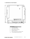

Diamond-MM-48-AT User Manual V1.01 Page 12
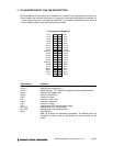
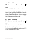
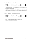
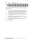
Base + 1 Read A/D MSB
Bit No. 7 6 5 4 3 2 1 0
Name AD15 AD14 AD13 AD12 AD11 AD10 AD9 AD8
Definitions:
AD15 – 8 A/D MSB data (bits 15-8 of the 16-bit value). A/D data is a signed 16-bit value
ranging from -32768 to 32767.
Note: Reading from Base + 0 and Base + 1 result in the same physical operation, reading
from the FIFO. The FIFO is 8 bits wide x 2048 bytes deep, with A/D data stored and retrieved
in interleaved fashion. Data from the A/D is put into the FIFO in little-endian mode, with the
LSB inserted first, and the MSB inserted second. Thus the data comes out of the FIFO in the
same order. Each time a byte is read from either Base + 0 or Base + 1, the next byte will be
read from the FIFO and the FIFO counter will be decremented.
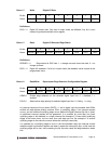
Because the FIFO decrements after each read operation, you cannot read out the same A/D
value more than once (unless the FIFO is empty, in which case the last byte may be read
indefinitely). It is the programmer’s responsibility to ensure that data is read out of the FIFO
properly so that appropriate LSB / MSB pairs are read out together.
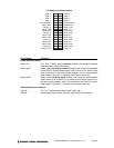
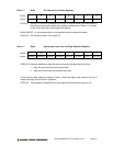
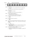
Base + 2 Read/Write A/D Channel Register
Bit No. 7 6 5 4 3 2 1 0
Name HIGH3 HIGH2 HIGH1 HIGH0 LOW3 LOW2 LOW1 LOW0
Definitions:
HIGH3 – 0 High channel of channel scan range; ranges from LOW to 15
LOW3 – 0 Low channel of channel scan range; ranges from 0 to 15
The high channel must be greater than or equal to the low channel.
When this register is written, the current A/D channel is set to the low channel and ADBUSY
= 1 for 10 uS. A/D channels are automatically selected in sequence by the board. Each time
an A/D conversion starts, the board increments to the next channel in the range. When the
high channel is sampled, the board resets to the low channel.