


Prometheus CPU User Manual V1.44 Page 33
11.3 Register Bit Definitions
In these register definitions, a bit marked ‘X’ is an unused bit.
All unused bits in readable registers read back as 0.
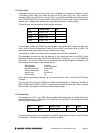
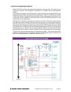
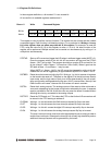
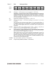
Base + 0 Write Command Register
Bit No. 7 6 5 4 3 2 1 0
Name STRTAD RSTBRD RSTDA RSTFIFO CLRDMA CLRT CLRD CLRA
This register is used to perform various functions. The register bits are not data bits but instead
command triggers. Each function is initiated by writing a 1 to a particular bit. Writing a 1 to any
bit in this register does not affect any other bit in this register. For example, to reset the
FIFO, write the value 0x10 (16) to this register to write a 1 to bit 4. No other function of the
register will be performed. Multiple actions can be carried out simultaneously by writing a 1 to
multiple bits simultaneously.
STRTAD Start an A/D conversion (trigger the A/D) when in software-trigger mode (AINTE = 0).
Once the program writes to this bit, the A/D conversion will start and the STS bit
(base + 3 bit 7) will go high. The program should then monitor STS and wait for it to
go low (check if value in base + 3 is less than 128 or 0x80). When it goes low the
A/D data at Base + 0 and Base + 1 may be read.
When AINTE = 1 (base + 4 bit 0), the A/D cannot be triggered by writing to this bit.
Instead the A/D will be triggered by a signal selected by ADCLK in base + 4 bit 5.
RSTBRD Reset the entire board excluding the D/A. Writing a 1 to this bit causes all registers
on the board to be reset to 0. The effect on the digital I/O is that all ports are reset to
input mode, and the logic state of their pins will be determined by the pull-up/pull-
down configuration setting selected by the user. All A/D, counter/timer, interrupt, and
DMA functions will cease. However the D/A values will remain constant.
RSTDA Reset the 4 analog outputs. The analog outputs will be reset to either mid-scale or
zero-scale, depending on the jumper configuration selected by the user. A separate
reset is provided for the D/A so that the user may reset the board if needed without
affecting the circuitry connected to the analog outputs.
RSTFIFO Reset the FIFO depth to 0. This clears the FIFO so that further A/D conversions will
be stored in the FIFO starting at address 0.
CLRDMA Writing a 1 to this bit causes the DMA interrupt request flip flop to be reset.
CLRT Writing a 1 to this bit causes the timer interrupt request flip flop to be reset.
CLRD Writing a 1 to this bit causes the digital I/O interrupt request flip flop to be reset.
CLRA Writing a 1 to this bit causes the analog interrupt request flip flop to be reset.
The user’s interrupt routine must write to the appropriate bit prior to exiting in order to
enable future interrupts. Otherwise the interrupt line will stay high indefinitely and no
additional interrupt requests will be generated by the board.