


Prometheus CPU User Manual V1.44 Page 49
14.4 Perform an A/D conversion on the current channel
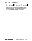
After the above steps are completed, start the A/D conversion by writing to Base + 0. This write
operation only triggers the A/D if AINTE = 0 (interrupts are disabled). When AINTE = 1, the A/D
can only be triggered by the on-board counter/timer or an external signal. This protects against
accidental triggering by software during a long-running interrupt-based acquisition process.
outp(base,0x80);
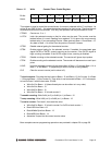
14.5 Wait for the conversion to finish
The A/D converter chip takes up to 5 microseconds to complete one A/D conversion. Most
processors and software can operate fast enough so that if you try to read the A/D converter
immediately after starting the conversion, you will beat the A/D converter and get invalid data.
Therefore the A/D converter provides a status signal to indicate whether it is busy or idle. This bit
can be read back as bit 7 in the status register at Base + 3. When the A/D converter is busy
(performing an A/D conversion), this bit is 1 and the program must wait. When the A/D converter
is idle (conversion is done and data is available), this bit is 0 and the program may read the data.
Here are examples:
while (inp(base+3) & 0x80); // Wait for conversion to finish before proceeding
This method could hang your program if there is a hardware fault and the bit is stuck at 1. Better
is to use a loop with a timeout:
int checkstatus() // returns 0 if ok, -1 if error
int i;
for (i = 0; i < 10000; i++)
{
if !(inp(base+3) & 0x80) then return(0); // conversion completed
}
return(-1); // conversion didn’t complete
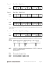
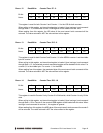
14.6 Read the data from the board
Once the conversion is complete, you can read the data back from the A/D converter. The data is
a 16-bit value and is read back in two 8-bit bytes. The LSB must be read from the board before
the MSB, because the data is inserted into the board’s FIFO in that order. Unlike other registers
on the board, the A/D data may only be read one time, since each time a byte is read from the
FIFO, the FIFO’s internal pointer advances, and that byte is no longer available. Note that
reading data from an empty FIFO returns unpredictable results.
The following pseudo-code illustrates how to read and construct the 16-bit A/D value:
LSB = inp(base);
MSB = inp(base+1);
Data = MSB * 256 + LSB; // combine the 2 bytes into a 16-bit value
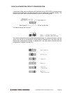
The final data is interpreted as a 16-bit signed integer ranging from –32768 to +32767.
⇒ Note: The data range always includes both positive and negative values, even if the board is
set to a unipolar input range. The data must now be converted to volts or other engineering units
by using a conversion formula as shown on the next page.
In scan mode, the behavior is the same except that when the program initiates a conversion, all
channels in the programmed channel range will be sampled once, and the data will be stored in
the FIFO. The FIFO depth register will increment by the scan size. When STS goes low, the
program should read out the data for all channels.