


EPSON Stylus PHOTO 810/820/830 Revision B
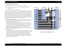
Operating Principles Electrical Circuit Operating Principles 44
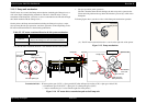
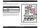
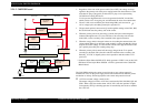
1. Regardless of the state of the power switch (On or OFF), the voltage is always
applied to the primary side of the power supply board from the moment or at the
state that AC-plug is plugged in. At this time, F1 plays a role of preventing
AC100V from coming into the F1.
L1 also prevents high harmonic wave noise generated in the RC circuit filter
which consists of C1 from going out, and eliminates the noise from outside here.
2. The AC is full-wave rectified by the diode bridge DB1, and converted to x
AC in voltage by the smoothing electrolytic capacitor C11.
3. The pressured up direct current turns Q1 on through the starting resistor R31 and
starts the primary side of the circuit.
4. When the primary side is On, the energy (current) led by the electromagnetic
induction through the trans (T1) does not flow to the secondary side since the
diode (D51) on the secondary side is installed in the opposite direction.
5. When the energy which is charged in the trans is reaching the saturated state, the
voltage which makes Q1 on becomes weak gradually. At the point that this voltage
drops at the certain voltage, C13 absorbs the current in the opposite direction and
Q1 is quickly shut off by the resulting sharp drop.
6. When the primary side is turned off, the energy charged in the T1 is opened
according to the diode (D51) direction which is installed on the secondary side.
Basically, 42 V DC is output by these circuit operations and the number of T1
spiral coil.
7. +5VDC is generated by pressured down this +42VDC as power supply. IC51
pressures down the +42VDC and generates precise +5VDC by chopping off the
output, forming the standard santooth wave form by the outer RC integration
circuit.
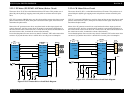
The C417 PSB/PSE board has the various control circuits to stop voltage output if a
malfunction occurs on the power supply board or the main board or while the printer
mechanism is on duty. Following explains each control and protection circuit.
+42V line constant voltage control circuit :
The output voltage level of the +42V line is monitored by R92, R93, Q91 and
ZD51. When +42V line reaches about +42.8V, PC1 starts the operation via Q91.
Consequently, FET Q1 switching operation is controlled by this circuit to stabilize
the +42V line.
+42Vline over voltage protection circuit :
The output voltage line is monitored by ZD52 and ZD87. If the output voltage
level of +42VDC line exceeds +48V, this circuit stops the operation of the
switching FET Q1 via PC1,Q82 and Q83, and prevents high voltage from being
applied to the secondary side.
+42VDC line drop limitation circuit :
PC1 drives with +36V and ZD90 is monitoring the voltage supplied to PC1. If the
supplied voltage level exceeds 37V, this circuit shuts down the +42V line
temporarily and prevents the over voltage from being applied to the PC1.
+42Vline over current protection circuit :
The output current level is monitored by the F51. When the abnormal current is
detected by F51, F51 blows and cuts off the +42V line output to the Main board.
+5V line constant voltage control circuit/+5V line over current protection circuit :
The output voltage level of the +5VDC line is monitored by the regulator IC51. If
abnormal voltage is detected, the information is fed back to the internal
comparator.
+5V line over voltage protection circuit :
The output voltage level of the +5VDC line is monitored by ZD53.
If the output voltage level of +5DC line exceeds +7V, this circuit stops the
operation of the switching FET Q1 via PC1,Q82 and Q83, and prevents high
voltage from being applied to the secondary side.
2