


4
■ F
2
MC-8L Family Features
• Minimum execution time: 0.32µs/12.5MHz, 0.4 µs/10MHz, 0.95 µs/4.2 MHz
• Operating voltage: +2.2 V to +6.0 V, operating frequency: 1 MHz to 10 MHz
• Software-switchable instruction cycle (4 speeds) provides low voltage, low-power comsumption operation (clock
gear function)
• Backup voltage in stop mode (voltage required to maintain RAM data): Min. +1.5 V
• Bitwise selectable pull-up resistors for each I/O port
• One-time PROM products support (by programming data) the same option settings as mask ROM products (the
option settings are mask options for some products).
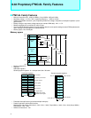
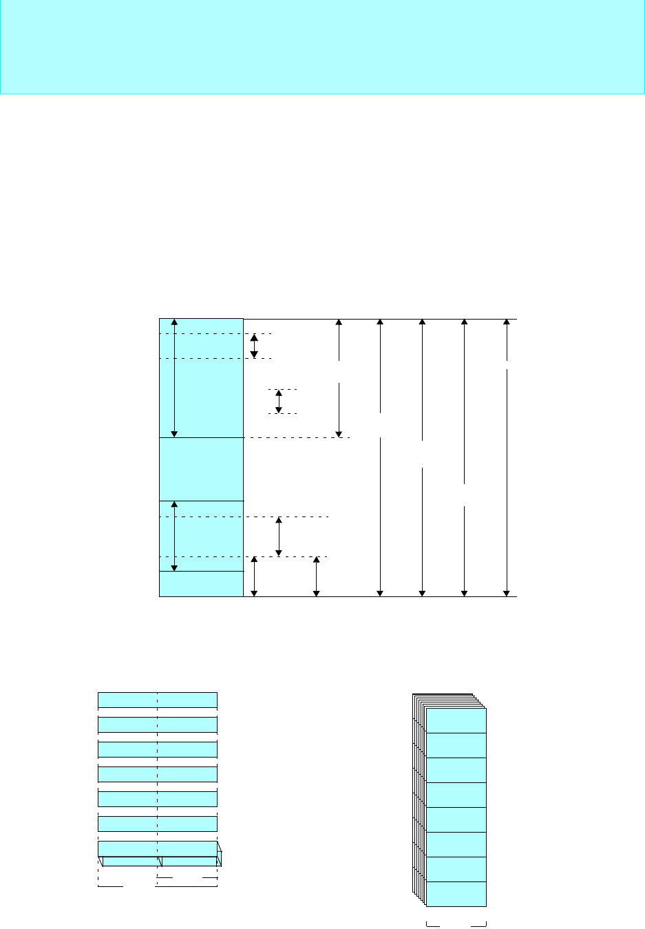
• Memory space: Max. 64 Kbytes
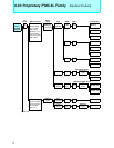
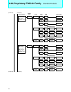
Memory space
• Memory mapped I/O
•Registers
Dedicated registers
General-purpose registers: 8 × 8-bit per bank, Max. 32 banks
• Enhanced interrupt function (prioritized multiple interrupts)
• Powerful operation and transfer functions
Multiplication and division instructions: 8-bit × 8-bit = 16-bit (7.6µs/10MHz), 16-bit ÷ 8-bit = 8-bit (8.4µs/10MHz)
Data transfer: Max. 16-bit
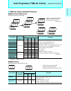
• Number of instructions: 136
Relative
addressing
Bit
direct
addressing
General-purpose
register addressing
Vector
addressing
FFFFH
FFD0H
FFC0H
0200H
0100H
0000H
+127
-128
Program
area
External
area
Data area
I/O area
Direct
addressing
Immediate
addressing
Extended
addressing
Pointer
addressing
64KB
Index
addressing
0100H+(RP × 8H) →
Lower address
Upper address
8 bits
General-purpose registers
Max. 32
AH
PC
IX
SP
EP
PS
AL
TH TL
Dedicated registers
Accumulator
Temporary accumulator
Program counter
Index register
Stack pointer
Extra pointer
Program status
Register bank pointer
Condition code register
8 bits
16 bits
RP CCR
R7
R6
R5
R4
R3
R2
R1
R0
8-bit Proprietary F
2
MC-8L Family Features