


Operation Theorem
•
31
4.2.1 A/D Conversion Procedure
The A/D conversion is starting by a trigger source, then the A/D converter
will start to convert the signal to a digital value. The PCI-9112 provides
three trigger modes, see section 5.1.2.
While A/D conversion, the DRDY bit in A/D status register is cleared to
indicate the data is not ready. After conversion being completed, the
DRDY bit will return to high(1) level. It means users can read the
converted data from the A/D data registers. Please refer section 4.5 for
the A/D status register format.
The A/D data should be transferred into PC's memory for further using.
The PCI-9112 provides three data transfer modes that allow users to
optimize the DAS system. Refer to section 5.1.3 for data transfer modes.
4.2.2 A/D Trigger Modes
In the PCI-9112, A/D conversion can be triggered by the Internal or
External trigger source. The EITS bit of A/D control register is used to
select the internal or external trigger, please refer to section 4.5 for details.
Whenever the external source is set, the internal sources are disable.
If the internal trigger is selected, there are two internal sources, the
software trigger and the timer pacer trigger can be used. The A/D
operation mode is controlled by A/D mode bits (EITS, TSTS) of A/D
control register (BASE+18). Total three trigger sources are possible in
the PCI-9112. The different trigger conditions are specified as follows:
Software trigger
The trigger source is software controllable in this mode. That is, the A/D
conversion is starting when any value is written into the software trigger
register (BASE+20). This trigger mode is suitable for low speed A/D
conversion. Under this mode, the timing of the A/D conversion is fully
controlled under software. However, it is difficult to control the fixed A/D
conversion rate except another timer interrupt service routine is used to
generate a fixed rate trigger.
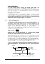
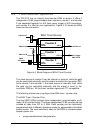
Timer Pacer Trigger
An on-board timer / counter chip 8254 is used to provide a trigger source
for A/D conversion at a fixed rate. Two counters of the 8254 chip are
cascaded together to generate trigger pulse with precise period. Please
refer to section 5.4 for 8254 architecture. This mode is ideal for high
speed A/D conversion. It can be combined with the DMA bus mastering or
the interrupt data transfer. It's recommend to use this mode if your
applications need a fixed and precise A/D sampling rate.