


36
•
Operation Theorem
Ø event counter
Ø binary rate multiplier
Ø real-time clock
Ø Digital one-shot
Ø motor control
For more information about the 8254, please refer to the NEC
Microprocessors and peripherals or Intel Microsystems Components
Handbook.
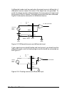
Pacer Trigger Source
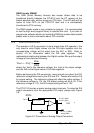
The counter 1 and counter 2 are cascaded together to generate the timer
pacer trigger of A/D conversion. The frequency of the pacer trigger is
software controllable. The maximum pacer signal rate is 2MHz/4=500K
which excess the maximum A/D conversion rate of the PCI-9112. The
minimum signal rate is 2MHz/65536/65536, which is a very slow
frequency that user may never use it.
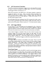
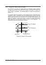
General Purpose Timer/ Counter
The counter 0 is free for users' applications. The clock source, gate
control signal and the output signal is send to the connector CN3. The
general purpose timer / counter can be used as event counter, or used for
measuring frequency, or others functions.
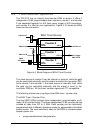
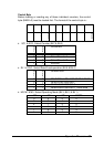
I/O Address
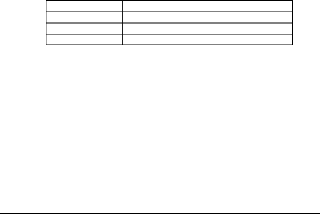
The 8254 in the PCI-9112 occupies 4 I/O address as shown below.
BASE + 0 LSB OR MSB OF COUNTER 0
BASE + 1 LSB OR MSB OF COUNTER 1
BASE + 2 LSB OR MSB OF COUNTER 2
BASE + 3 CONTROL BYTE
The programming of 8254 is control by the registers BASE+0 to BASE+3.
The functionality of each register is specified this section. For more
detailed information, please refer handbook of 8254 chip.