


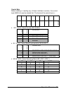

Operation Theorem
•
33
DMA Transfer (DMAX)
The DMA (Direct Memory Access) bus master allows data to be
transferred directly between the PCI-9112 and the PC memory at the
fastest possible rate, without using any CPU time. The A/D data will be
queue at local FIFO on the PCI-9112 itself and it is automatically
transferred to PC's memory.
The DMA transfer mode is very complex to program. It is recommended
to use the high level program library to operate this card. If you wish to
program the software which can handle the DMA bus master data transfer,
please refer to more information about PCI controller.
4.3 D/A Conversion
The operation of D/A conversion is more simple than A/D operation. You
only need to write Digital values into the D/A data registers and the
corresponding voltage will be output from the AO1 or AO2. Refer to
section 4.3 for information about the D/A data registers. The
mathematical relationship between the Digital number DAn and the output
voltage is formulated as following:
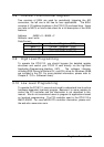
Vout Vref
DAn
= − ×
4096
where the Vref is the reference voltage, the Vout is the output voltage,
and the DAn is the Digital value in D/A data registers.
Before performing the D/A conversion, users should care about the D/A
reference voltage which set by the JP3 and JP4. Please refer section 2.8
for jumper setting. The reference voltage will effect the output voltage. If
the reference voltage is -5V, the D/A output scaling will be 0~5V. If the
reference voltage is -10V, the D/A output scaling will be 0~10V.
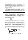
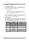
The PCI-9112 has two unipolar analog output channels. To make the D/A
output connections from the appropriate D/A output, please refer Figure
3.8.
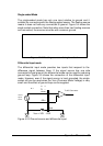
To D/A Output
D/A Converter
Ref In
-5 or -10
INT or Ext
Analog GND
Pin-30 ( AO0)
Pin-32 ( AO1)
Pin-14 ( A.GND)
Figure 4.3 Connection of Analog Output Connection
D/A