


Operation Theorem
•
35
4.5 Timer/Counter Operation
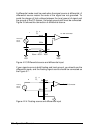
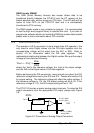
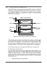
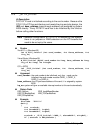
The PCI-9112 has an interval timer/counter 8254 on board. It offers 3
independent 16-bit programmable down counters; counter 1 and counter
2 are cascaded together for A/D timer pacer trigger of A/D conversion,
and counter 0 is free for your applications. Figure 3.10 shows the 8254
timer/counter connection.
Counter 0
Counter 1
Counter 2
CLK0
GATE0
OUT0
CLK1
GATE1
CLK2
GATE2
OUT1
OUT2
2MHz
Oscillator
Vcc
A/D Trigger
CN3 Pin-34
CN3 Pin-37
CN3 Pin-33
CN3 Pin-16
CN3 Pin-35
INT
EXT
8254 Timer/Counter
Figure 4.5 Block Diagram of 8254 Timer/Counter
The clock source of counter 0 can be internal or external, while the gate
can be controlled externally and the output is send to the connector CN3.
As to counter 0 and counter 1, the clock source is internally fixed, while
the gate can be controlled externally and the output is send to the
connector CN3 too. All the timer/ counter signals are TTL compatible.
The following shows how to configure the 8254 timer / counter chip.
The 8254 Timer / Counter Chip
The Intel (NEC) 8254 contains three independent, programmable, multi-
mode 16 bit counter/timers. The three independent 16 bit counters can be
clocked at rates from DC to 5 MHz. Each counter can be individually
programmed with 6 different operating modes by appropriately formatted
control words. The most commonly uses for the 8254 in microprocessor
based system are:
Ø programmable baud rate generator