


EM78P447N
8-Bit Microcontroller with OTP ROM
6 •
Product Specification (V1.1) 03.30.2005
(This specification is subject to change without further notice)
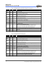
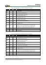
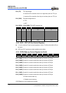
Table 5 EM78P447NDK and EM78P447NDM Pin Description
Symbol Pin No. Type Function
VDD 3 - ■ Power supply.
OSCI 19 I
■ XTAL type: Crystal input terminal or external clock input pin.
■ RC type: RC oscillator input pin.
OSCO 18 I/O
■ XTAL type: Output terminal for crystal oscillator or external clock input pin.
■ RC type: Instruction clock output.
■ External clock signal input.
TCC 2 I
■ The real time clock/counter (with Schmitt trigger input pin) must be tied to
VDD or VSS if not in use.
/RESET 20 I
■ Input pin with Schmitt trigger. If this pin remains at logic low, the controller
will also remain in reset condition.
P50~P54 6~9,1 I/O ■ P50~P54 are bi-directional I/O pins.
P60 10 I/O
■ P60 are bi-directional I/O pins. This can be pulled-high internally by
software control.
P71~P77 11~17 I/O
■ P74~P77 are bi-directional I/O pins.
■ P74~P75 can be pulled-high internally by software control.
■ P76~P77 can have open-drain output by software control.
■ P71 can also be defined as the R-option pins.
/INT 5 I ■ External interrupt pin triggered by falling edge.
VSS 4 - ■ Ground.
NC 3 - ■ No connection.
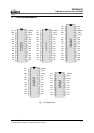
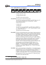
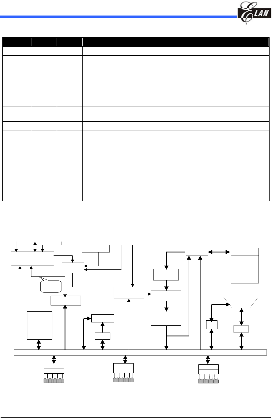
4 FUNCTION DESCRIPTION
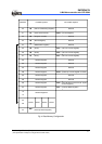
IOC5
R5
P
5
0
P
5
1
P
5
2
P
5
3
P
5
4
P
5
5
P
5
6
P
5
7
IOC6
R6
IOC7
R7
ACC
R3
STACK 1
STACK 2
STACK 3
STACK 4
STACK 5
P C
ROM
Instruction
Register
Instruction
Decoder
ALU
Interrupt
Control
R4
RAM
WDT Timer
Prescale
r
Oscillator/Timing
Control
WDT
Time-out
R1(TCC)
Sleep
&
Wake
Control
DATA & CONTROL BUS
/INTTCC
OSCI
OSCO
/RESET
P
6
0
P
6
1
P
6
2
P
6
3
P
6
4
P
6
5
P
6
6
P
6
7
P
7
0
P
7
1
P
7
2
P
7
3
P
7
4
P
7
5
P
7
6
P
7
7
Fig. 2 Functional Block Diagram