


EM78P447N
8-Bit Microcontroller with OTP ROM
Product Specification (V1.1) 03.30.2005
• 13
(This specification is subject to change without further notice)
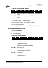
4.2.5 IOCE (WDT Control Register)
7 6 5 4 3 2 1 0
- ODE WDTE SLPC ROC - - /WUE
Bit 6 (ODE) Control bit is used to enable the open-drain of P76 and P77 pins
0: Disable open-drain output.
1: Enable open-drain output.
The ODE bit can be read and written.
Bit 5 (WDTE) Control bit used to enable Watchdog timer.
The WDTE bit is useful only when ENWDT, the CODE Option bit, is "0".
It is only when the ENWDT bit is "0" that WDTE bit. is able to
disabled/enabled the WDT.
0: Disable WDT.
1: Enable WDT.
The WDTE bit is not used if ENWDT, the CODE Option bit ENWDT, is
"1". That is, if the ENWDT bit is "1", WDT is always disabled no matter
what the WDTE bit status is.
The WDTE bit can be read and written.
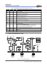
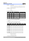
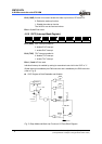
Bit 4 (SLPC) This bit is set by hardware at the low level trigger of wake-up signal and
is cleared by software. SLPC is used to control the oscillator operation.
The oscillator is disabled (oscillator is stopped, and the controller enters
into SLEEP2 mode) on the high-to-low transition and is enabled
(controller is awakened from SLEEP2 mode) on low-to-high transition.
In order to ensure the stable output of the oscillator, once the oscillator is
enabled again, there is a delay for approximately 18ms
1
(oscillator
start-up timer, OST) before the next instruction of the program is
executed. The OST is always activated by a wake-up event from sleep
mode regardless of the Code Option bit ENWDT status is "0" or
otherwise. After waking up, the WDT is enabled if the Code Option
ENWDT is "1". The block diagram of SLEEP2 mode and wake-up
invoked by an input trigger is depicted in Fig. 5. The SLPC bit can be
read and written.
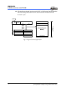
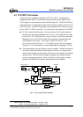
Bit 3 (ROC) ROC is used for the R-option. Setting ROC to "1" will enable the status
of R-option pins (P70, P71) for the controller to read. Clearing ROC will
disable the R-option function. Otherwise, the R-option function is
introduced. Users must connect the P71 pin or/and P70 pin to VSS with
a 430KΩ external resistor (Rex). If Rex is connected/disconnected with
VDD, the status of P70 (P71) will be read as "0"/"1" (refer to Fig. 7(b)).
The ROC bit can be read and written.
1
<Note>: Vdd = 5V, set up time period = 16.2ms ± 30%
Vdd = 3V, set up time period = 19.6ms ± 30%