


Contents
Product Specification (V1.1) 03.30.2005 • iii
Contents
1 GENERAL DESCRIPTION ......................................................................................... 1
2 FEATURES ................................................................................................................. 1
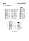
3 PIN ASSIGNMENT ..................................................................................................... 3
4 FUNCTION DESCRIPTION ........................................................................................ 6
4.1 Operational Registers......................................................................................... 7
4.1.1 R0 (Indirect Addressing Register) .......................................................................7
4.1.2 R1 (Time Clock /Counter)....................................................................................7
4.1.3 R2 (Program Counter) & Stack ...........................................................................7
4.1.4 R3 (Status Register)..........................................................................................10
4.1.5 R4 (RAM Select Register).................................................................................10
4.1.6 R5~R7 (Port 5 ~ Port7) .....................................................................................10
4.1.7 R8~R1F and R20~R3E (General Purpose Register)........................................10
4.1.8 R3F (Interrupt Status Register) .........................................................................11
4.2 Special Purpose Registers ............................................................................... 11
4.2.1 A (Accumulator).................................................................................................11
4.2.2 CONT (Control Register)...................................................................................11
4.2.3 IOC5 ~ IOC7 (I/O Port Control Register) ..........................................................12
4.2.4 IOCB (Wake-up Control Register for Port6)......................................................12
4.2.5 IOCE (WDT Control Register)...........................................................................13
4.2.6 IOCF (Interrupt Mask Register).........................................................................14
4.3 TCC/WDT & Prescaler ..................................................................................... 15
4.4 I/O Ports ........................................................................................................... 16
4.5 RESET and Wake-up ....................................................................................... 17
4.5.1 RESET ..............................................................................................................17
4.5.2 The Status of RST, T, and P of STATUS Register.............................................21
4.6 Interrupt ............................................................................................................22
4.7 Oscillator .......................................................................................................... 23
4.7.1 Oscillator Modes................................................................................................23
4.7.2 Crystal Oscillator/Ceramic Resonators(XTAL)..................................................24
4.7.3 External RC Oscillator Mode.............................................................................25
4.8 CODE Option Register .....................................................................................26
4.8.1 Code Option Register (Word 0).........................................................................26
4.8.2 Customer ID Register (Word 1).........................................................................28
4.9 Power On Considerations ................................................................................ 28
4.10 External Power On Reset Circuit...................................................................... 28
4.11 Residue-Voltage Protection.............................................................................. 29
4.12 Instruction Set .................................................................................................. 30
4.13 Timing Diagram ................................................................................................ 33