


© Copyright IBM Corp. 2006. All rights reserved. 25
Chapter 2. Architecture and technical
overview
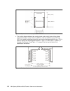
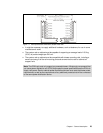
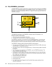
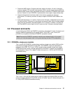
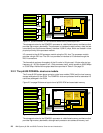
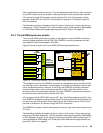
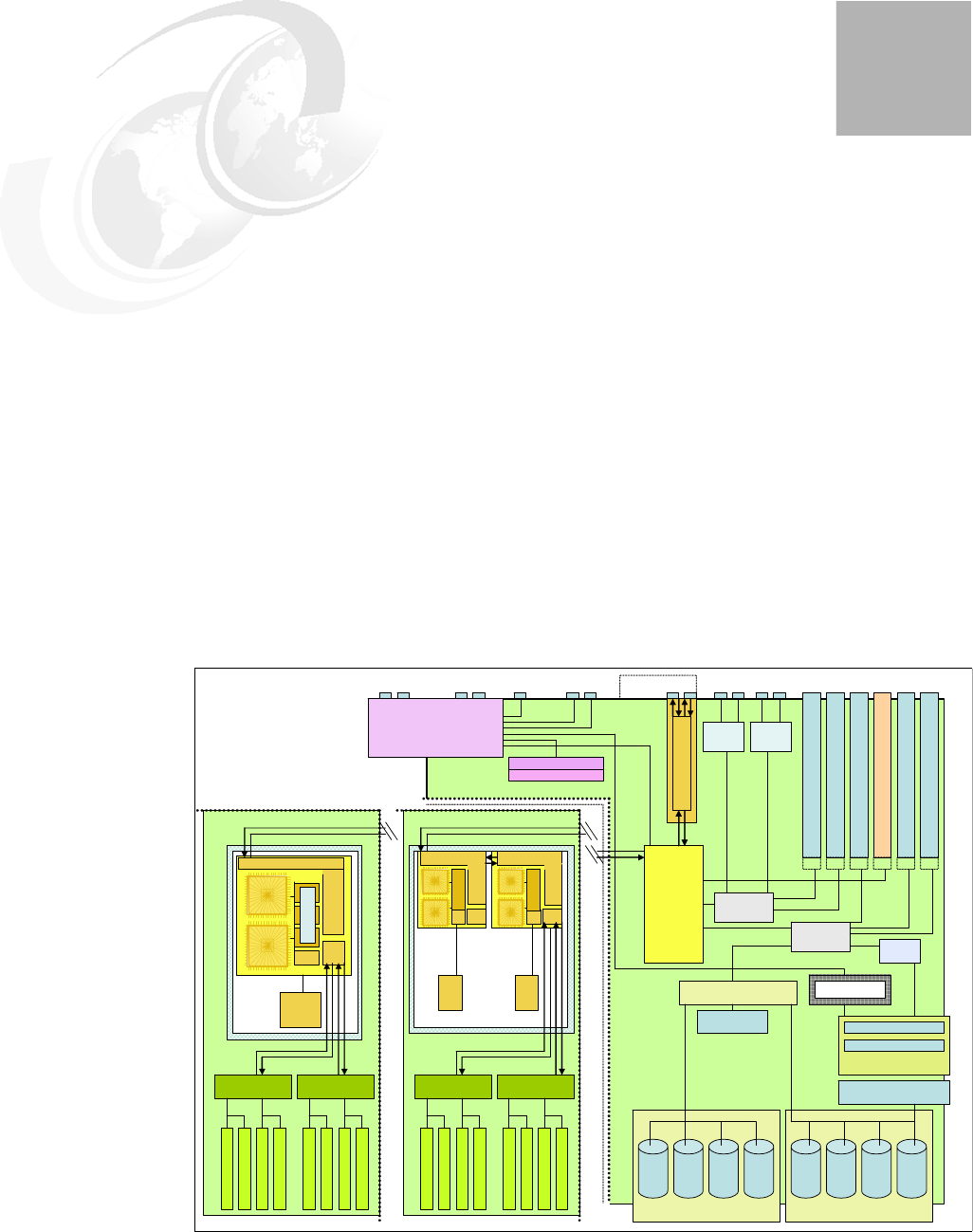
This chapter discusses the overall system architecture of the p5-520 and p5-520Q. Figure 2-1
details the base system hardware and the DCM or QCM options. (You cannot mix an
installation of DCM and QCM options.) The bandwidths in this chapter are theoretical
maximums that are provided for reference. We always recommend that you obtain real-world
performance measurements using production workloads.
Figure 2-1 IBM System p5 520 and IBM System p5 520Q architecture with QCM or DCM
2
Enhanced
I/O Controller
GX+
700
MHz
(DCM)
Remote I/O card
RIO-2 bus 2B (Diff’l)
Each direction @ 1GB/s
Service Processor
Two SPCN ports
P1-C7-T3 T4
System Ports
P1-T1 T2
HMC ports
P1-C7-T1 T2
Rack Indicator Light
cable port P1-T9
CoD key card
buzz interface
USB ports
P1-T7 T8
Ethernet ports
P1-T5 T6
USB
32-bit
Dual 1GB
Ethernet
64-bit
PCI-X slot 1, 64-bit, 133 MHz, 3.3 volts
PCI-X slot 2, 32-bit, 66 MHz, 3.3 volts
PCI-X slot 3, 32-bit, 66 MHz, 3.3 volts
PCI-X slot 4, 64-bit, 266 MHz, 3.3 volts
PCI-X slot 5, 64-bit, 133 MHz, 3.3 volts
Short Long LongShort Short
PCI-X to PCI-X
bridge 0
133
MHz
33
MHz
PCI-X to PCI-X
bridge 3
IDE
controller
133 MHz 64-bit
Dual SCSI
Ultra320 64-bit
RAID enablement
card
4-pack disk drive backplane
P2-T15-L15-L0
4-pack disk drive backplane
P3-T14-L15-L0
Tape drive
P4-D1
Optional media backplane
Slim-line media device
Slim-line media device
Operator panel
P1-C1C2C3C4C5
P2-T11-L8-L0
P2-T11-L5-L0
P2-T11-L4-L0
P2-T11-L3-L0
P2-D1
P2-D2
P2-D3
P2-D4
P3-D1
P3-D2
P3-D3
P3-D4
P3-T11-L8-L0
P3-T11-L5-L0
P3-T11-L4-L0
P3-T11-L3-L0
2x4 B @
633 MHz
66 MHz
32-bit
POWER5+
core
2.1 GHz
POWER5+
core
2.1 GHz
POWER5+
core
2.1 GHz
POWER5+
core
2.1 GHz
1.9 MB Shared
L2 cache
L3
Ctrl
Mem
Ctrl
DCM
Enhanced distributed
switch
SMI-II SMI-II
1056 MHz
2x8 B for read
2x8 B for write
DIMM CX JXX “Ax”
DIMM CX JXX “Ax”
DIMM CX JXX “Ax”
DIMM CX JXX “Ax”
DIMM CX JXX “Ax”
DIMM CX JXX “Ax”
DIMM CX JXX “Ax”
DIMM CX JXX “Ax”
2x8 B
@528 MHz
36 MB
L3 cache
2x16 B
@1.05 GHz
QCM
2x16B
@825 MHz
SMI-II SMI-II
1056 MHz
2x8 B for read
2x8 B for write
DIMM CX JXX “Ax”
DIMM CX JXX “Ax”
DIMM CX JXX “Ax”
DIMM CX JXX “Ax”
DIMM CX JXX “Ax”
DIMM CX JXX “Ax”
DIMM CX JXX “Ax”
DIMM CX JXX “Ax”
36 MB
L3 cache
2x16B
@825 MHz
36 MB
L3 cache
Core
1.65 GHz
Core
1.65 GHz
1.9 MB
L2 cache
1.9 MB
L2 cache
L3
ctrl
L3
ctrl
Mem
ctrl
Mem
ctrl
Enhanced
distributed switch
Enhanced
distributed switch
Core
1.65 GHz
Core
1.65 GHz
To Enhanced I/O ControllerTo Enhanced I/O Controller
PCI-X slot 6, 64-bit, 133 MHz, 3.3 volts
Long
C6
2x8 B
@528 MHz