


28 IBM System p5 520 and 520Q Technical Overview and Introduction
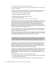
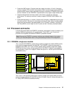
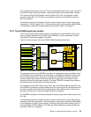
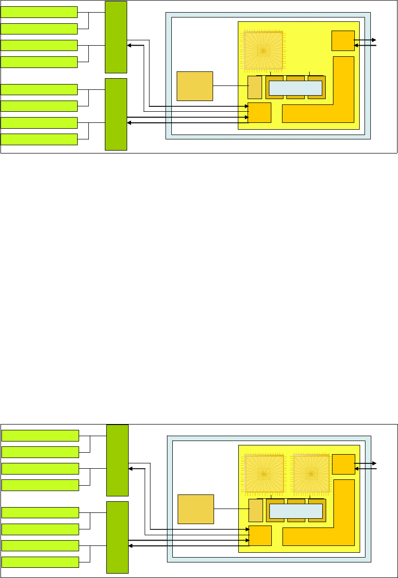
Figure 2-4 p5-520 POWER5+ 2.1 GHz SCM with DDR2 memory socket layout view
The storage structure for the POWER5+ processor is a distributed memory architecture that
provides high-memory bandwidth. The processor is interfaced to eight memory slots that are
controlled by two Synchronous Memory Interface II (SMI-II) chips, which are located in close
physical proximity to the processor module.
I/O connects to the p5-520 processor module using the GX+ bus. The processor module
provides a single GX+ bus. The GX+ bus provides an interface to I/O devices through the
RIO-2 connections.
The theoretical maximum throughput of the L3 cache is 16 byte read, 16 byte write at a bus
frequency of 1.05 GHz (based on a 2.1 GHz processor clock), which equates to 33600 MBps
or 33.60 GBps. Additional throughput details are provided in Table 2-3 on page 33.
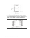
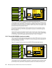
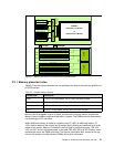
2.2.2 The p5-520 POWER5+ dual-core module
The 2-core p5-520 system planar contains a dual-core module (DCM) and the local memory
storage subsystem for that DCM. The POWER5+ dual-core processor and its associated L3
cache are packaged in the DCM.
Figure 2-5 on page 28 shows a layout view of p5-520 DCM and associated memory.
Figure 2-5 The p5-520 POWER5+ 2.1 GHz DCM with DDR2 memory socket layout view
The storage structure for the POWER5+ processor is a distributed memory architecture that
provides high-memory bandwidth, although each processor can address all memory and
POWER5+
core
1.9 MB Shared
L2 cache
L3
Ctrl
Mem
Ctrl
36 MB
L3 cache
Single-Core Module
SCM
2x16B
2:1
SMI-II SMI-II
1056 MHz
2 x 8 B for read
2 x 2 B for write
DIMM
DIMM
DIMM
DIMM
DIMM
DIMM
DIMM
DIMM
2 x 8 B
@528 MHz
GX+
Ctrl
Enhanced distributed switch
GX+
Bus
POWER5+
core
POWER5+
core
1.9 MB Shared
L2 cache
L3
Ctrl
Mem
Ctrl
36 MB
L3 cache
Single-Core Module
SCM
2x16B
2:1
SMI-II SMI-II
1056 MHz
2 x 8 B for read
2 x 2 B for write
DIMM
DIMM
DIMM
DIMM
DIMM
DIMM
DIMM
DIMM
2 x 8 B
@528 MHz
GX+
Ctrl
Enhanced distributed switch
GX+
Bus
POWER5+
core
2.1 GHz
POWER5+
core
2.1 GHz
1.9 MB Shared
L2 cache
L3
Ctrl
Mem
Ctrl
36 MB
L3 cache
DCM
2x16B
@1.05 GHz
SMI-II SMI-II
1056 MHz
2 x 8 B for read
2 x 2 B for write
DIMM
DIMM
DIMM
DIMM
DIMM
DIMM
DIMM
DIMM
2 x 8 B
@528 MHz
GX+
Ctrl
Enhanced distributed switch
GX+
Bus
POWER5+
core
2.1 GHz
POWER5+
core
2.1 GHz
POWER5+
core
2.1 GHz
POWER5+
core
2.1 GHz
1.9 MB Shared
L2 cache
L3
Ctrl
Mem
Ctrl
36 MB
L3 cache
DCM
2x16B
@1.05 GHz
SMI-II SMI-II
1056 MHz
2 x 8 B for read
2 x 2 B for write
DIMM
DIMM
DIMM
DIMM
DIMM
DIMM
DIMM
DIMM
2 x 8 B
@528 MHz
GX+
Ctrl
Enhanced distributed switch
GX+
Bus