


Intel
®
8500 Chipset North Bridge (NB) and eXternal Memory 11
Bridge (XMB) Thermal/Mechanical Design Guide
2 Packaging Technology
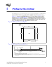
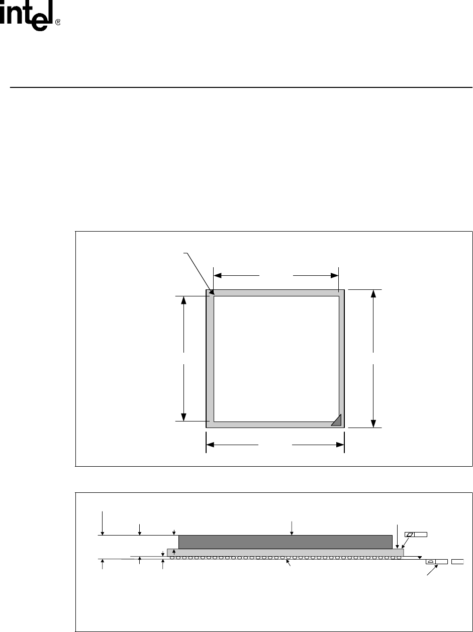
The E8500 chipsets consist of four individual components: the NB, the XMB, the Intel
®
6700PXH
64-bit PCI Hub and the I/O controller hub (ICH5r). The E8500 chipset NB component use a
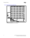
42.5 mm squared, 12-layer flip chip ball grid array (FC-BGA) package (see Figure 2-1 through
Figure 2-3). The E8500 chipset XMB component uses a 37.5mm squared, 10-layer FB-BGA
package (see Figure 2-4 through Figure 2-6). For information on the Intel 6700PXH 64-bit PCI
Hub package, refer to the Intel
®
6700PXH 64-bit PCI Hub Thermal/Mechanical Design Guide. For
information on the ICH5 package, refer to the Intel
®
82801EB I/O Controller Hub 5 (ICH5) and
Intel
®
82801ER I/O Controller Hub 5 R (ICH5R) Thermal Design Guide.
Figure 2-1. NB Package Dimensions (Top View)
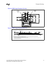
Figure 2-2. NB Package Dimensions (Side View)
TNB
IHS
42.5 mm
42.5 mm38.5 mm
38.5 mm
Handling
Exclusion
Area
NB
IHS
0.20 –C–
IHS
Substrate
0.435 ± 0.025 mm
See Note 3
Seating Plane
2.44 ± 0.071 mm
See Note 1
Notes:
1. Primary datum -C- and seating plan are defined by the spherical crowns of the solder balls (shown before motherboard attach)
2. All dimensions and tolerances conform to ANSI Y14.5M-1994
3. BGA has a pre-SMT height of 0.5mm and post-SMT height of 0.41-0.46mm
4. Shown before motherboard attach; FCBGA has a convex (dome shaped) orientation before reflow and is expected to have a slightly concave (bowl shaped)
orientation after reflow
0.20
See Note 4
3.79 ± 0.144 mm
4.23 ± 0.146 mm