


Intel
®
8500 Chipset North Bridge (NB) and eXternal Memory 13
Bridge (XMB) Thermal/Mechanical Design Guide
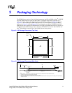
Packaging Technology
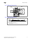
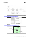
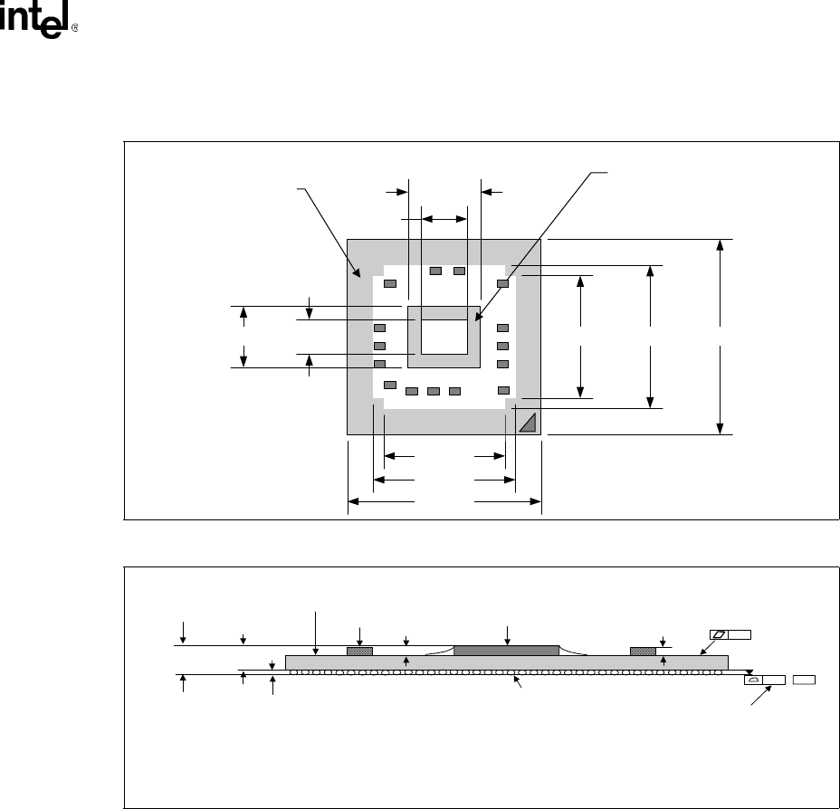
Figure 2-4. XMB Package Dimensions (Top View)
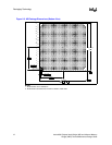
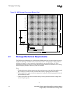
Figure 2-5. XMB Package Dimensions (Side View)
XMB
Die
Die
Keepout
Area
Handling
Exclusion
Area
37.50mm.27.50mm.23.50mm.
37.50mm.
27.50mm.
23.50mm.
14.02mm.
8.88mm.
6.65mm.11.73mm.
Notes:
1. Primary datum -C- and seating plan are defined by the spherical crowns of the solder balls (shown before motherboard attach)
2. All dimensions and tolerances conform to ANSI Y14.5M-1994
3. BGA has a pre-SMT height of 0.5mm and post-SMT height of 0.41-0.46mm
4. Shown before motherboard attach; FCBGA has a convex (dome shaped) orientation before reflow and is expected to have a slightly concave
(bowl shaped) orientation after reflow
0.20
–C–
Die
Substrate
0.435 ± 0.025 mm
See Note 3
Seating Plane
2.100 ± 0.121 mm
See Note 1
Decoup
Cap
0.7 mm Max
2.535 ± 0.123 mm
0.84 ± 0.05 mm
0.20
See Note 4