


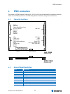
4 ETX® connectors
Kontron User's Guide ETX CD 26
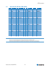
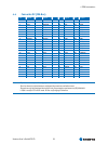
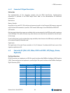
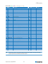
4.4.2 Connector X2 Signal Description
ISA Bus Slot
The implementation of this subsystem complies with the ETX® Specification. Implementation
information is provided in the ETX® Design Guide. Refer to the documentation for additional
information.
Restrictions:
Memory Transfer:
According to the used LPC 2 ISA solution only memory transfer in the Firmware HUB memory range and
with Firmware HUB commands is possible. The Firmware HUB range is from FED4:0000 to FED4:0FFF
I/O Transfer:
Only two generic decoding ranges are available which can be selected in the BIOS setup with a maximum
size of 256 Byte. This works of course only, when there are no other devices connected to that I/O ports
in that range.
It can be that there is only one decoding range available, when there are the COM and/or parallel ports
of an external SuperI/O controller used.
Signal level:
The signal level of the used Fintec controller is 3,3V, 5V tolerant. To achieve the 5V level, most of the
signals are pulled up to 5V.
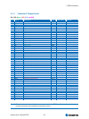
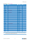
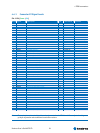
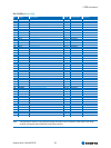
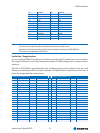
4.5 Connector X3 (VGA, LCD, Video, COM1 and COM2, LPT/Floppy, Mouse,
Keyboard)
Flat-Panel Interfaces
ETX®-CD modules can implement an LVDS flat-panel interface called JUMPtec Intelligent LVDS Interface
(JILI). These modules do not implement a parallel digital flat-panel interface called JUMPtec Intelligent
Digital Interface (JIDI).
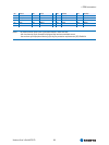
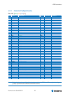
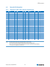
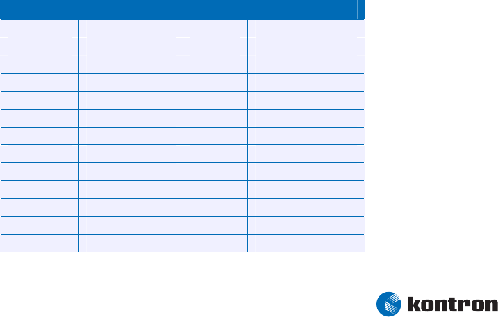
LVDS Interface Pinout (JILI)
Pin Signal Pin Signal
1 GND 2 GND
3 R 4 B
5 HSY 6 G
7 VSY 8 DDCK
9 DETECT#** 10 DDDA
11 LCDDO16 12 LCDDO18
13 LCDDO17 14 LCDDO19
15 GND 16 GND
17 LCDDO13 18 LCDDO15
19 LCDDO12 20 LCDDO14
21 GND 22 GND
23 LCDDO8 24 LCDDO11