


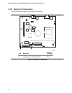

Technical Reference
45
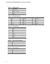
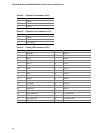
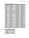
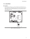
Table 28. PCI Bus Connector (J4B1)
Pin Signal Pin Signal Pin Signal Pin Signal
A1 Ground (TRST#)* B1 -12 V A32 AD16 B32 AD17
A2 +12 V B2 Ground (TCK)* A33 +3.3 V B33 C/BE2#
A3 +5 V (TMS)* B3 Ground A34 FRAME# B34 Ground
A4 +5 V (TDI)* B4 No connect (TDO)* A35 Ground B35 IRDY#
A5 +5 V B5 +5 V A36 TRDY# B36 +3.3 V
A6 INTA# B6 +5 V A37 Ground B37 DEVSEL#
A7 INTC# B7 INTB# A38 STOP# B38 Ground
A8 +5 V B8 INTD# A39 +3.3 V B39 LOCK#
A9 Reserved B9 No connect (PRSNT1#)* A40 Reserved B40 PERR#
A10 +5 V (I/O) B10 Reserved A41 Reserved B41 +3.3 V
A11 Reserved B11 No connect (PRSNT2#)* A42 Ground B42 SERR#
A12 Ground B12 Ground A43 PAR B43 +3.3 V
A13 Ground B13 Ground A44 AD15 B44 C/BE1#
A14 +3.3 V aux B14 Reserved A45 +3.3 V B45 AD14
A15 RST# B15 Ground A46 AD13 B46 Ground
A16 +5 V (I/O) B16 CLK A47 AD11 B47 AD12
A17 GNT# B17 Ground A48 Ground B48 AD10
A18 Ground B18 REQ# A49 AD09 B49 Ground
A19 PME# B19 +5 V (I/O) A50 Key B50 Key
A20 AD30 B20 AD31 A51 Key B51 Key
A21 +3.3 V B21 AD29 A52 C/BE0# B52 AD08
A22 AD28 B22 Ground A53 +3.3 V B53 AD07
A23 AD26 B23 AD27 A54 AD06 B54 +3.3 V
A24 Ground B24 AD25 A55 AD04 B55 AD05
A25 AD24 B25 +3.3 V A56 Ground B56 AD03
A26 IDSEL B26 C/BE3# A57 AD02 B57 Ground
A27 +3.3 V B27 AD23 A58 AD00 B58 AD01
A28 AD22 B28 Ground A59 +5 V (I/O) B59 +5 V (I/O)
A29 AD20 B29 AD21 A60 REQ64C# B60 ACK64C#
A30 Ground B30 AD19 A61 +5 V B61 +5 V
A31 AD18 B31 +3.3 V A62 +5 V B62 +5 V
* These signals (in parentheses) are optional in the PCI specification and are not currently implemented.
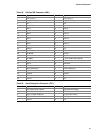
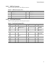
Table 29. ATAPI CD-ROM Connector (J2D1)
Pin Signal Name
1 Left audio input from CD-ROM
2 CD audio differential ground
3 CD audio differential ground
4 Right audio input from CD-ROM