Technical Product Specification 19
Order #273817
Intel NetStructure
®
MPCBL0001 High Performance Single Board Computer
Contents
2.2.2 Chipset
The Intel
®
E7501 chipset consists of three major components:
• Intel
®
E7501 Memory Controller Hub (MCH)
• Intel
®
82801CA I/O Controller Hub 3 (ICH3)
• Intel
®
82870P2 64-bit PCI/PCI-X Controller Hub 2 (P64H2)
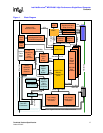
See Figure 20, “Component Layout (#1)” on page 100 for their locations.
2.2.2.1 Intel
®
E7501 Memory Controller Hub (U22)
The Intel
®
E7501 Memory Controller Hub (MCH) interfaces between the processor system bus
and the memory and I/O subsystems.
Significant features are listed below:
• System/host bus features:
— Supports dual processors at either 400 or 533 MT/s or a bandwidth of 3.2 or 4.3 GBytes/s
— Supports a 36-bit system bus addressing model
— 12 deep in-order queue, two deep defer queue
Note: The current MPCBL0001 is designed to run with the Intel
®
LV Xeon
®
2.0 GHz processor. At this
processor frequency, the processor side bus (PSB) will run at 400 MT/s with a bandwidth of 3.2
GBytes/s.
• Memory subsystem features:
— 144-bit wide (72-bit x 2), DDR-266 memory interfaces with 3.2 or 4.3 GByte/s bandwidth
— Supports x72, registered DDR-266 ECC DIMMs using 64-, 128-, 256-, and 512-Mbit
SDRAMs
— Supports a maximum of 16 GBytes of memory (MPCBL0001 SBC implementation
supports a maximum of 8 Gbytes).
— Supports S4EC/D4ED ChipKill* ECC (x4 ChipKill)
• Corrects all bit errors within a single 4-bit nibble
• Detects all errors contained within two 4-bit nibbles
• Memory scrubbing supported
— Supports up to 32 simultaneous open pages
— Hardware support for auto-initialization of memory with valid ECC
• I/O features:
— Hub interface A provides HI 1.5 connection for ICH3
• 266 MB/s data bandwidth with parity protection
• 8 bits wide, 66 MHz clock, 4x data transfer (quad-pumped)
• Supports 64-bit inbound addressing, 32-bit outbound addressing
— Hub interfaces B and C provide HI2.0 connections for two P64H2s
• 1 GByte/s data bandwidth with ECC protection in each direction


