


CONTENTS
Chapter 1. INTRODUCTION
1.1 Features·································································································································································1-1
1.2 Terminology··························································································································································1-2
1.2.1 Analog Value : A ··················································································································································1-2
1.2.2 Digital Value : D ···················································································································································1-2
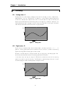
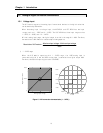
1.3 Analog to Digital Conversion Characteristics ····················································································1-3
1.3.1 Voltage input························································································································································1-3
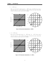
1.3.2 Current input························································································································································1-5
Chapter 2. SPECIFICATIONS
2.1 General Specifications ··································································································································2-1
2.2 Performance Specifications ·······················································································································2-2
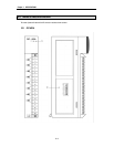
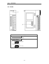
2.3 Names of Parts and Functions ··················································································································2-4
2.3.1 G3F-AD3A ·························································································································································2-4
2.3.2 G4F-AD3A ·························································································································································2-5
2.3.3 G6F-AD2A ·························································································································································2-6
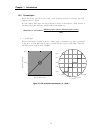
2.4 I/O Conversion Characteristics ·················································································································2-7
2.4.1 Voltage Input Characteristics ··························································································································2-8
2.4.2 Current Input Characteristics ··························································································································2-10
2.4.3 Simultaneous Voltage and Current Input Characteristics ················································································2-11
2.4. 4 Analog input and Digital output characteristics ·······························································································2-12
2.5 Processing Specification······························································································································2-13
2.5.1 Sampling processing A/D conversion system···································································································2-13
2. 5.2 Averaging processing A/D conversion system ·································································································2-13
Chapter 3. INSTALLATION AND WIRING
3.1 Installation ··························································································································································3-1
3.1.1 Installation Ambience··········································································································································3-1
3.1.2 Handling Precautions ········································································································································3-1