


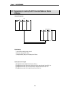

Chapter 6 Buffer memory
6 - 6
6.2.2 G3F-AD3A / G4F-AD3A
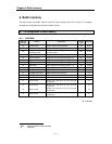
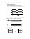
1) Channel enable (Address 00)
- When the power is on, all bits are set as 0 (off) and all channels are disabled.
- In order to enable a channel, set the corresponding bit as 1 (on). For example, turn on
the bit 2 to enable the channel 2.
- Because the conversion time depends on the number of used channel, turning on just
necessary channel can reduce A/D conversion time.
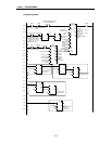
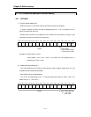
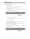
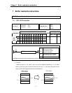
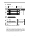
bit15 bit14 bit13 bit12 bit11 bit10 bit9 bit8 bit7 bit6 bit5 bit4 bit3 bit2 bit1 bit0
– – – – – – – – Ch7 Ch6 Ch5 Ch4 Ch3 Ch2 Ch1 Ch0
Example) To enable channel 1, 2, and 3 for G4F-AD3A :
Write h000D ( turn on bit 1, 2, and 3 ) to buffer 00, and sampling time is
obtained as 3 × 5ms = 15ms.
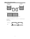
2) Input voltage/current type (Address 01)
- This function is available with G3F-AD3A and G4F-AD3A. With the G6F-AD2A, the input
voltage/current type isn’t set by sequence program.
- Turn on the cor responding bit as ‘1’ to set the input voltage/current type as 0 ~ 10 VDC.
The default value is ‘0’ ( 1 ~ 5 VDC and DC4~20mA ).
- When use current input, be sure to set the corresponding bit as ‘0’. Otherwise, the
module will not operate normally.
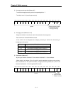
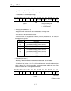
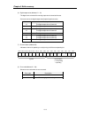
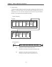
bit15 bit14 bit13 bit12 bit11 bit10 bit9 bit8 bit7 bit6 bit5 bit4 bit3 bit2 bit1 bit0
– – – – – – – – Ch7 Ch6 Ch5 Ch4 Ch3 Ch2 Ch1 Ch0
Channel enable
0 : A/D conversion disable
1 : A/D conversion enable
Ignored
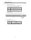
Assign input voltage range
0 : 1 ~ 5 VDC and DC4~20mA
1 : 0 ~ 10 VDC
Ignored