


DS33Z41 Quad IMUX Ethernet Mapper
23 of 167
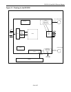
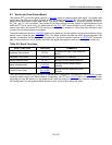
8.1 Processor Interface
Microprocessor control of the DS33Z41 is accomplished through the 20 interface pins of the microprocessor port.
The 8-bit parallel data bus can be configured for Intel or Motorola modes of operation with the two MODEC[1:0]
pins. When MODEC[1:0] = 00, bus timing is in Intel mode, as shown in Figure 11-11
and Figure 11-12. When
MODEC[1:0] = 01, bus timing is in Motorola mode, as shown in Figure 11-13
and Figure 11-14. The address
space is mapped through the use of 8 address lines, A0 - A7. Multiplexed Mode is not supported on the processor
interface.
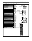
The Chip Select (CS) pin must be brought to a logic low level to gain read and write access to the microprocessor
port. With Intel timing selected, the Read (RD) and Write (WR) pins are used to indicate read and write operations
and latch data through the interface. With Motorola timing selected, the Read-Write (RW) pin is used to indicate
read and write operations while the Data Strobe (DS) pin is used to latch data through the interface.
The interrupt output pin (INT) is an open-drain output that will assert a logic-low level upon a number of software
maskable interrupt conditions. This pin is normally connected to the microprocessor interrupt input. The register
map is shown in Table 9-1
.
8.1.1 Read-Write/Data Strobe Modes
The processor interface can operate in either read-write strobe mode or data strobe mode. When MODEC[1:0] =
00 the read-write strobe mode is enabled and a negative pulse on RD performs a read cycle, and a negative
pulse on WR performs a write cycle. When MODEC[1:0] pins = 01 the data strobe mode is enabled and a
negative pulse on DS when RW is high performs a read cycle, and a negative pulse on DS when RW is low
performs a write cycle. The read-write strobe mode is commonly called the “Intel” mode, and the data strobe
mode is commonly called the “Motorola” mode.
8.1.2 Clear on Read
The latched status registers will clear on a read access. It is important to note that in a multi-task software
environment, the user should handle all status conditions of each register at the same time to avoid inadvertently
clearing status conditions. The latched status register bits are carefully designed so that an event occurrence
cannot collide with a user read access.
8.1.3 Interrupt and Pin Modes
The interrupt (INT) pin is configurable to drive high or float when not active. The INTM bit controls the pin
configuration, when it is set the INT pin will drive high when not active. After reset, the INT pin is in high
impedance mode until an interrupt source is active and enabled to drive the interrupt pin.