


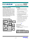

DS33Z41 Quad IMUX Ethernet Mapper
5 of 167
LIST OF FIGURES
Figure 3-1. Quad T1/E1 SCT to DS33Z41 .............................................................................................................. 11
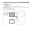
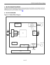
Figure 6-1. Detailed Block Diagram......................................................................................................................... 13
Figure 7-1. DS33Z41 256-Ball CSBGA Pinout........................................................................................................ 21
Figure 8-1. Clocking for the DS33Z41..................................................................................................................... 25
Figure 8-2. Device Interrupt Information Flow Diagram .......................................................................................... 30
Figure 8-3. IMUX Interface to T1/E1 Transceivers.................................................................................................. 32
Figure 8-4. Diagram of Data Transmission with IMUX Operation ........................................................................... 32
Figure 8-5. Command Structure for IMUX Function................................................................................................ 34
Figure 8-6. Flow Control Using Pause Control Frame ............................................................................................ 41
Figure 8-7. IEEE 802.3 Ethernet Frame.................................................................................................................. 42
Figure 8-8. Configured as DTE Connected to an Ethernet PHY in MII Mode......................................................... 44
Figure 8-9. DS33Z41 Configured as a DCE in MII Mode........................................................................................ 45
Figure 8-10. RMII Interface...................................................................................................................................... 47
Figure 8-11. MII Management Frame...................................................................................................................... 48
Figure 8-12. PRBS Synchronization State Diagram................................................................................................ 49
Figure 8-13. Repetitive Pattern Synchronization State Diagram............................................................................. 50
Figure 8-14. LAPS Encoding of MAC Frames Concept .......................................................................................... 55
Figure 8-15. X.86 Encapsulation of the MAC field .................................................................................................. 56
Figure 8-16. CIR in the WAN Transmit Path ........................................................................................................... 59
Figure 10-1. MII Transmit Functional Timing......................................................................................................... 140
Figure 10-2. MII Transmit Half Duplex with a Collision Functional Timing............................................................ 140
Figure 10-3. MII Receive Functional Timing.......................................................................................................... 141
Figure 10-4. RMII Transmit Interface Functional Timing....................................................................................... 141
Figure 10-5 RMII Receive Interface Functional Timing......................................................................................... 141
Figure 11-1. Transmit MII Interface ....................................................................................................................... 144
Figure 11-2. Receive MII Interface Timing ............................................................................................................ 145
Figure 11-3. Transmit RMII Interface..................................................................................................................... 146
Figure 11-4. Receive RMII Interface Timing.......................................................................................................... 147
Figure 11-5. MDIO Timing ..................................................................................................................................... 148
Figure 11-6. Transmit WAN Timing....................................................................................................................... 149
Figure 11-7. Receive WAN Timing........................................................................................................................ 150
Figure 11-8. SDRAM Interface Timing .................................................................................................................. 152
Figure 11-9. Receive IBO Channel Interleave Mode Timing................................................................................. 153
Figure 11-10. Transmit IBO Channel Interleave Mode Timing.............................................................................. 154
Figure 11-11. Intel Bus Read Timing (MODEC = 00)............................................................................................ 156
Figure 11-12. Intel Bus Write Timing (MODEC = 00)............................................................................................ 156
Figure 11-13. Motorola Bus Read Timing (MODEC = 01) .................................................................................... 157
Figure 11-14. Motorola Bus Write Timing (MODEC = 01)..................................................................................... 157
Figure 11-15. JTAG Interface Timing Diagram ..................................................................................................... 158
Figure 12-1. JTAG Functional Block Diagram....................................................................................................... 159
Figure 12-2. TAP Controller State Diagram .......................................................................................................... 162
Figure 12-3. JTAG Functional Timing.................................................................................................................... 165