


The P4X4-ALH Mainboard
Page 31
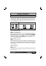
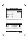
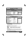
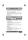
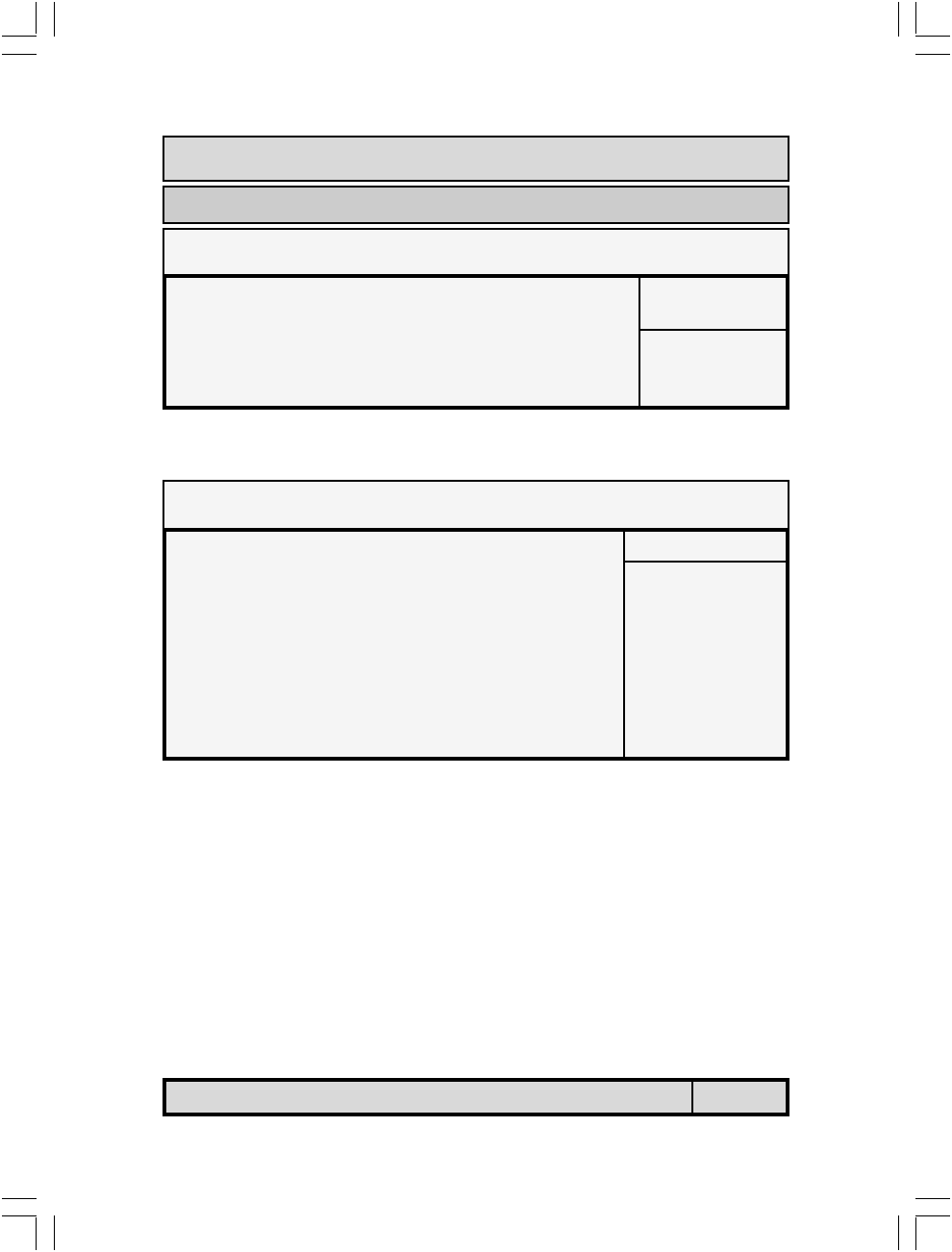
Dram Clock Drive Control
This field allows you to select the FSB and DRAM frequency. When you press
enter the following menu will appear.
Managing The PC BIOS
4DRAM Clock/Drive Control
4AGP & P2P Bridge Control
4CPU & PCI Bus Control
Memory Hole
System BIOS Cacheable
Video RAM Cacheable
Delay Prior To Thermal
Item Help
Menu Level 4
Phoenix - AwardBIOS CMOS Setup Utility
Advanced Chipset Features
[Press Enter]
[Press Enter]
[Press Enter]
[Disabled]
[Disabled]
[Disabled]
[16 Min]
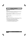
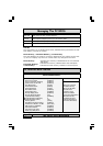
3.5. Advanced Chipset Features
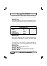
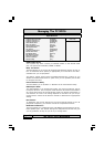
Current FSB Frequency
Current DRAM Frequency
DRAM Clock
DRAM Timing
X SDRAM CAS Latency
X Bank Interleave
X Precharge to Active (Trp)
X Active to Precharge (Tras)
X Active to CMD (Trcd)
XDRAM Command Rate
DRAM Burst Len
Write Recovery Time
Item Help
Menu Level 44
Phoenix - AwardBIOS CMOS Setup Utility
DRAM Clock/Drive Control
100 MHz
133 MHz
[By SPD]
[By SPD]
3
[Disabled]
3T
7T
3T
2T Command
[4]
[3T]
4Current FSB Frequency
The setting for this field will be automatically selected by the BIOS.
4Current Dram Frequency
The setting for this field will be automatically detected by the BIOS. The
value that is selected in derived from the RAM clock.
4DRAM Clock
When you press enter you will have three options:
By SPD :The BIOS will automatically detect the actual DRAM Clock.
100 MHz :The DRAM clock speed will be PC1600 (100 MHz DDR).
133 MHz :The DRAM clock speed will be PC2100 (133 MHz DDR).
166MHz :The DRAM clock speed will be PC2700 (166 MHz DDR).
4DRAM Timing
This field enables/disables you from selecting the values for following six
fields manually. These (six) fields determine the DRAM read/write timing. If
you select By SPD then those fields will be automatically configured by the
system BIOS. (The performance parameters of the installed memory chips
(DRAM) determines the value in those fields.)