Chapter 2 Connecting Signals
© National Instruments Corporation 2-11 SCXI-1141/1142/1143 User Manual
Analog Output Signal Connections
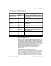
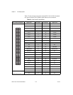
Pins 3 through 17 of the rear signal connector are analog output signal pins.
Pin 3 is the main output, and pin 4 is its reference signal. All eight channels
are multiplexed onto this output when the module is software-configured
for multiplexed scanning mode. In parallel scanning mode, the output of
pin 3 is the output of one selected channel. Channel 0 is the power-up and
reset default. When scanning multiple modules, you can also connect this
output to the SCXIbus analog bus and the analog bus will drive this output.
Pins 5, 7, 9, 11, 13, 15, and 17 are direct outputs from channels 1 through 7,
respectively. In parallel mode, all eight channels are available
simultaneously at the rear connector. Pins 6, 8, 10, 12, 14, 16, and 18 are
the reference signals for outputs 1 through 7.
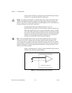
Caution The SCXI-1141/1142/1143 module analog outputs are not overvoltage protected,
although they are short-circuit protected. Applying external voltage to these outputs can
result in damage to the SCXI-1141/1142/1143 module. NI is not liable for any damage
resulting from such signal connections.
Digital I/O Signal Connections
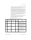
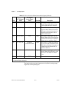
Pins 24 through 27, 29, 33, 36, 37, and 43 constitute the digital I/O lines
of the rear signal connector. Each of these pins is in one of three
categories—digital input signals, digital output signals, and timing signals.
Pins 24 and 33 are the digital ground reference for all of the DAQ device
digital signals and are tied to the module digital ground.
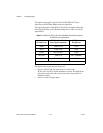
The digital input signals are pins 25, 27, 29, and 37. Each digital line
emulates an SCXIbus communication signal as follows:
• Pin 25 is SER DAT IN and is equivalent to the SCXIbus MOSI serial
data input line.
• Pin 27 is DAQ D*/A and is equivalent to the SCXIbus D*/A line.
Pin 27 indicates to the module whether the incoming serial stream on
SER DAT IN is data (DAQ D*/A = 0) or address (DAQ D*/A = 1)
information.
• Pin 29 is SLOT 0 SEL* and is equivalent to the SCXIbus INTR* line.
Pin 29 indicates whether the data on the SER DAT IN line is being sent
to Slot 0 (SLOT 0 SEL* = 0) or to a module (SLOT 0 SEL* = 1).
• Pin 37 is SER CLK and is equivalent to the SCXIbus SPI CLK line.
Pin 37 is used to clock the serial data on the SER DAT IN line into the
module registers.


