


NI 6509 User Guide and Specifications 6 ni.com
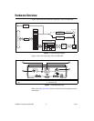
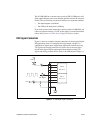
Hardware Overview
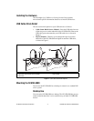
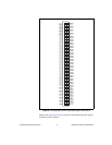
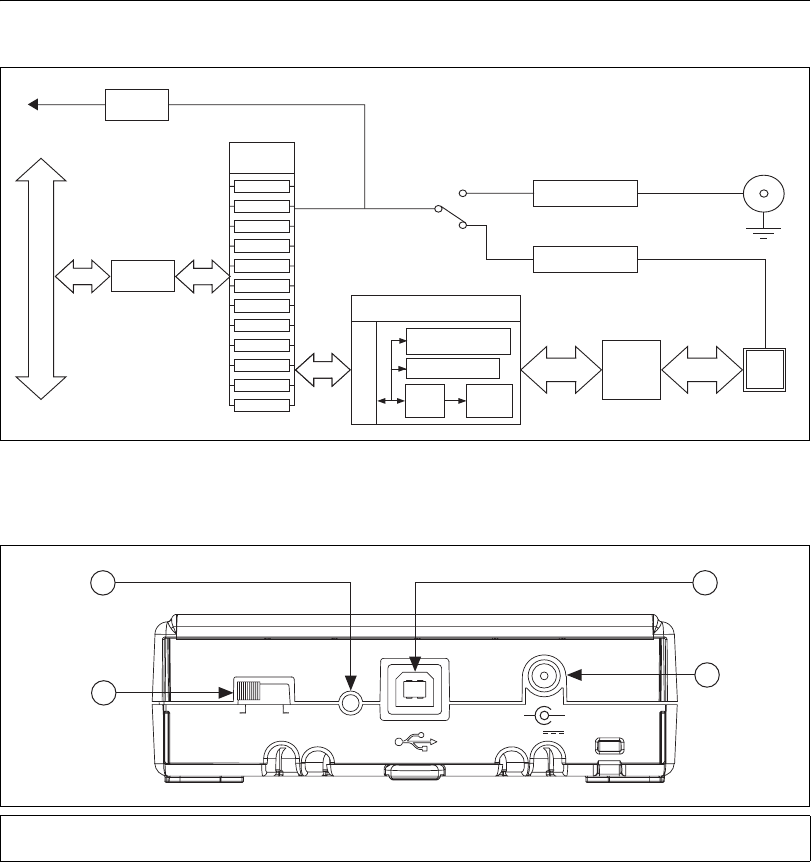
Figure 4 shows the key functional components of the NI USB-6509.
Figure 4. NI USB-6509 Block Diagram
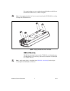
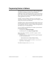
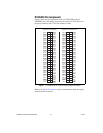
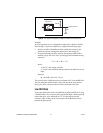
Figure 5 shows the back panel of the NI USB-6509.
Figure 5. NI USB-6509 Back Panel
Refer to the Safety Guidelines section of this document for important safety
information.
1 I/O Line Pull Switch
2LED
3 Recessed USB Port
4 DC Power Jack
Industrial Digital
I/O Control FPGA
DIO Lines
Programmable
Power-Up States
Watchdog Timer
Change
Detection
Digital
Filtering
USB
Interface
Data/Control
Port 0
Port 1
Port 2
Port 3
Port 4
Port 5
Port 6
Port 7
Port 8
Port 9
Port 10
Port 11
24 mA DIO
Tr anceivers
USB Data
12 V to 5 V
Regulation
VBUS Current
Sense
USB
Port
External Power
VBUS Power
I/O
Protection
96 DIO96 DIO96 DIO96 DIO
96 DIO96 DIO
96 DIO96 DIO
I/O Connector
Fuse and
Filter
+5 V
12 VDC Input
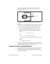
I/O LINE PULL
HIGH
LOW
12VDC
, 1A
+–
1
2
3
4