


Philips Semiconductors
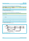
ISP1521
Hi-Speed USB hub controller
Product data Rev. 03 — 24 November 2004 36 of 53
9397 750 13702
© Koninklijke Philips Electronics N.V. 2004. All rights reserved.
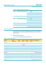
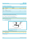
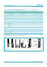
[1] All pins are 5 V tolerant.
[2] The bus capacitance (C
b
) is specified in pF. To meet the specification for V
OL
and the maximum rise time (300 ns), use an external
pull-up resistor with R
max
= 850/C
b
kΩ and R
min
=(V
CC
− 0.4)/3 kΩ.
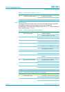
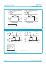
Table 38: Static characteristics: I
2
C-bus interface block
V
CC
= 3.0 V to 3.6 V; T
amb
=
−
40
°
Cto+70
°
C; unless otherwise specified.
Symbol Parameter Conditions Min Typ Max Unit
Input pin SCL and input/output pin SDA
[1]
V
IL
LOW-level input voltage - - 0.9 V
V
IH
HIGH-level input voltage 2.1 - - V
V
hys
hysteresis voltage 0.15 - - V
V
OL
LOW-level output voltage - - 0.4 V
t
f
output fall time V
IH
to V
IL
10<C
b
=10pFto400pF
[2]
- 0 250 ns
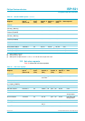
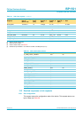
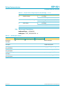
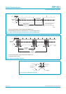
Table 39: Static characteristics: USB interface block (DP0 to DP7 and DM0 to DM7)
V
CC
= 3.0 V to 3.6 V; T
amb
=
−
40
°
Cto+70
°
C; unless otherwise specified.
Symbol Parameter Conditions Min Typ Max Unit
Input levels for high-speed
V
HSSQ
squelch detection threshold
(differential signal amplitude)
squelch detected - - 100 mV
no squelch detected 150 - - mV
V
HSCM
data signaling common-mode
voltage range
−50 - +500 mV
Output levels for high-speed
V
HSOI
idle state −10 - +10 mV
V
HSOH
data signaling HIGH 360 - 440 mV
V
HSOL
data signaling LOW −10 - +10 mV
V
CHIRPJ
chirp J level (differential voltage)
[1]
700 - 1100 mV
V
CHIRPK
chirp K level (differential voltage)
[1]
−900 - −500 mV
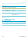
Input levels for full-speed and low-speed
V
IL
LOW-level input voltage - - 0.8 V
V
IH
HIGH-level input voltage (drive) 2.0 - - V
V
IHZ
HIGH-level input voltage (floating) 2.7 - 3.6 V
V
DI
differential input sensitivity |DP − DM| 0.2 - - V
V
CM
differential common-mode range 0.8 - 2.5 V
Output levels for full-speed and low-speed
V
OL
LOW-level output voltage 0 - 0.3 V
V
OH
HIGH-level output voltage 2.8 - 3.6 V
V
CRS
output signal crossover point
voltage
[2]
1.3 - 2.0 V
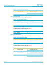
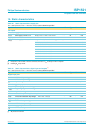
Leakage current
I
LZ
OFF-state leakage current −1- +1µA
Capacitance
C
IN
transceiver capacitance pin to GND - - 20 pF