


Philips Semiconductors
ISP1521
Hi-Speed USB hub controller
Product data Rev. 03 — 24 November 2004 49 of 53
9397 750 13702
© Koninklijke Philips Electronics N.V. 2004. All rights reserved.
20. Soldering
20.1 Introduction to soldering surface mount packages
This text gives a very brief insight to a complex technology. A more in-depth account
of soldering ICs can be found in our
Data Handbook IC26; Integrated Circuit
Packages
(document order number 9398 652 90011).
There is no soldering method that is ideal for all surface mount IC packages. Wave
soldering can still be used for certain surface mount ICs, but it is not suitable for fine
pitch SMDs. In these situations reflow soldering is recommended. In these situations
reflow soldering is recommended.
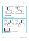
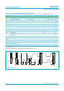
20.2 Reflow soldering
Reflow soldering requires solder paste (a suspension of fine solder particles, flux and
binding agent) to be applied to the printed-circuit board by screen printing, stencilling
or pressure-syringe dispensing before package placement. Driven by legislation and
environmental forces the worldwide use of lead-free solder pastes is increasing.
Several methods exist for reflowing; for example, convection or convection/infrared
heating in a conveyor type oven. Throughput times (preheating, soldering and
cooling) vary between 100 and 200 seconds depending on heating method.
Typical reflow peak temperatures range from 215 to 270 °C depending on solder
paste material. The top-surface temperature of the packages should preferably be
kept:
• below 225 °C (SnPb process) or below 245 °C (Pb-free process)
– for all BGA, HTSSON..T and SSOP..T packages
– for packages with a thickness ≥ 2.5 mm
– for packages with a thickness < 2.5 mm and a volume ≥ 350 mm
3
so called
thick/large packages.
• below 240 °C (SnPb process) or below 260 °C (Pb-free process) for packages with
a thickness < 2.5 mm and a volume < 350 mm
3
so called small/thin packages.
Moisture sensitivity precautions, as indicated on packing, must be respected at all
times.
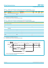
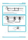
20.3 Wave soldering
Conventional single wave soldering is not recommended for surface mount devices
(SMDs) or printed-circuit boards with a high component density, as solder bridging
and non-wetting can present major problems.
To overcome these problems the double-wave soldering method was specifically
developed.
If wave soldering is used the following conditions must be observed for optimal
results:
• Use a double-wave soldering method comprising a turbulent wave with high
upward pressure followed by a smooth laminar wave.