


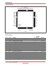
HD49335NP/HNP
Rev.1.0, Feb.12.2004, page 10 of 29
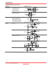
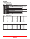
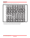
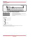
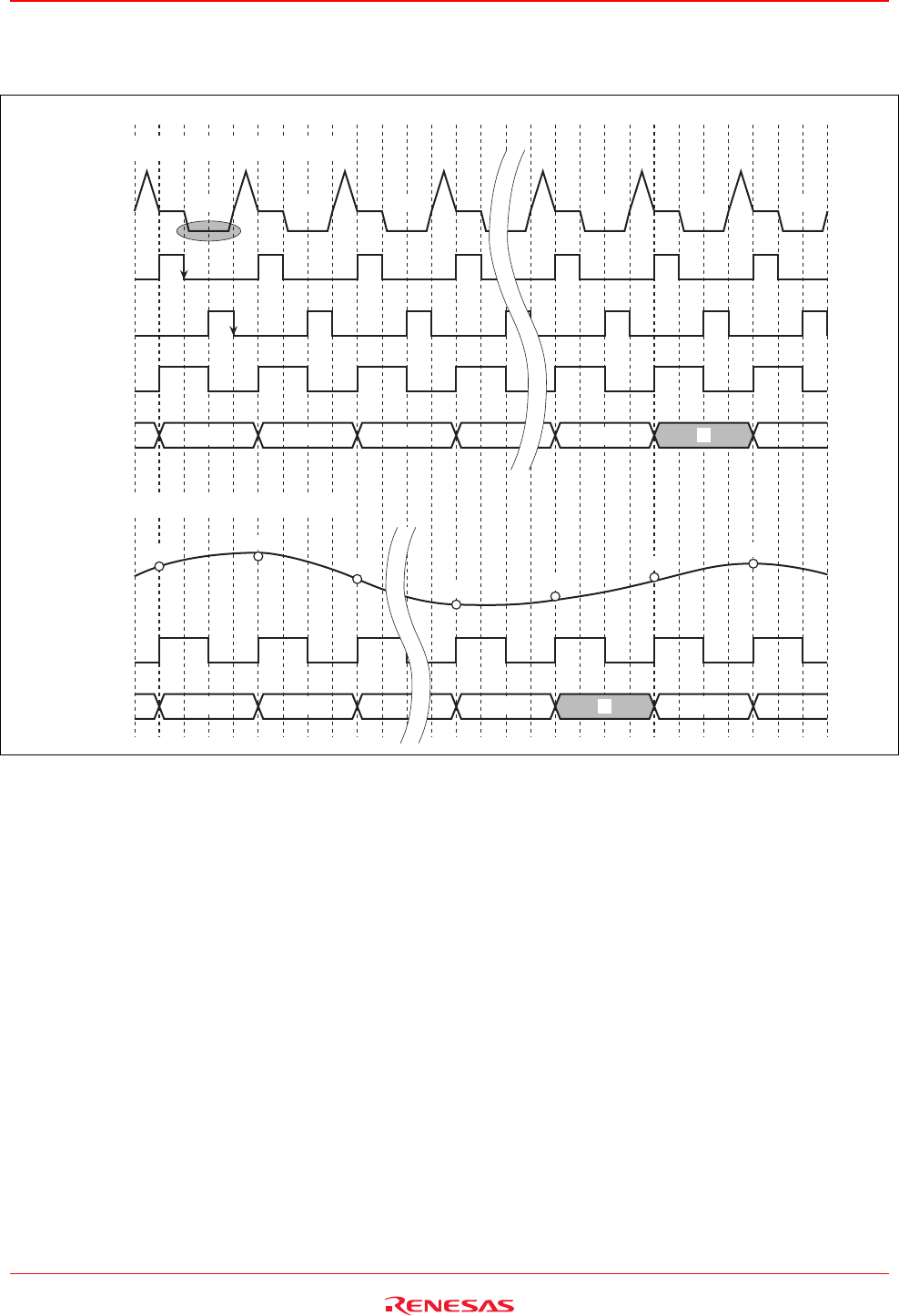
Timing Chart
Figure 2 shows the timing chart when CDSIN and ADCIN input modes are used.
012 91011
N+1 N+2 N+9 N+10 N+11N
CDS_in
SP1
SP2
ADCLK
D0 to D9
N+2
N+8
N+9
N+10
N+11
N−8N−9N−1
ADC_in
ADCLK
D0 to D9
N N+1
N
N+1
N−9N−8N−1 NN−10
• When CDS_in input mode is used
• When ADC_in input mode is used
~
Figure 2 Output Timing Chart when CDSIN and ADCIN Input Modes are Used
• The ADC output (D0 to D9) is output at the rising edge of the ADCLK in both modes.
• Pipe-line delay is ten clock cycles when CDSIN is used and nine when ADCIN is used.
• In ADCIN input mode, the input signal is sampled at the rising edge of the ADCLK.