


HD49335NP/HNP
Rev.1.0, Feb.12.2004, page 20 of 29
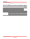
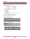
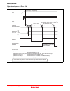
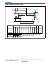
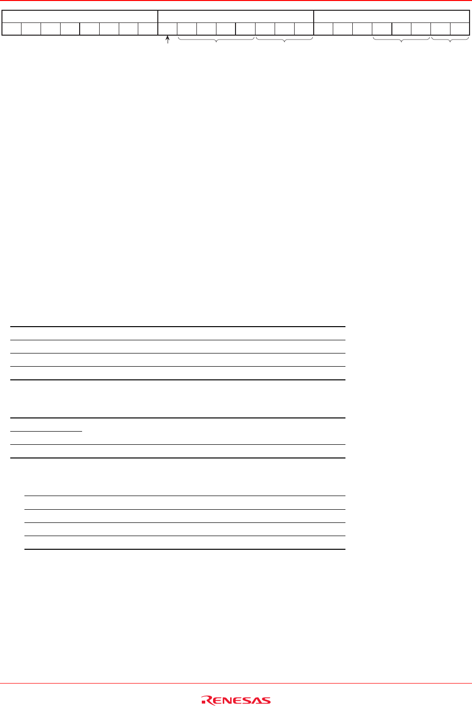
Address STD1[7:0] (L) STD2[15:8] (H)
11110100 D4D3D2D7 D6 D5 D1 D0 D12 D11 D10 D9 D8
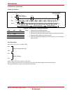
Gray_test
VD latch MON
Gray code
H12_Buff
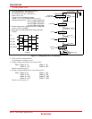
• MON (D0 to D2 of address H’F4)
Select the pulse which output to pin MON (pin 60).
When D0 to D2: 0, Fix to Low When 1, ADCLK
When 2, SP1 When 3, SP2
When 4, OBP When 5, PBLK
When 6, CPDM When 7, DLL_test
• H12Baff (D3 to D6 of address H’F4)
Select the buffer size which output to pin H1A, H2A (pin 22, 26).
D3: 2 mA buffer
D4: 4 mA buffer
D5: 10 mA buffer
D6: 14 mA buffer
Above data can be on/off individually. Default is D6 can be on only. (18 mA buffer)
• VD latch (D7 of address H’F4)
Data = 0: Gain data is determined when CS rising
Data = 1: Gain data is determined when VD falling
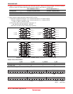
Differential Code and Gray Code (D8 to D12 of address H’F4)
• Gray code (D8 to D9 of address H’F4)
DC output code can be change to following type.
Gray Code [1] Gray Code [0] Output Code
0 0 Binary code
0 1 Gray code
1 0 Differential encoded binary
1 1 Differential encoded gray
• Serial data setting items (D10 to D12 of address H’F4)
Setting Bit Setting Contents
Gray_test[0]
Gray_test[1]
Standard data output timing control signal
(Refer to the following table)
Gray_test[2] ADCLK polar with OBP. (Lo→Positive edge, HI→Negative edge)
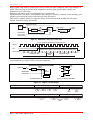
• Standard data output timing
Gray_test[1] Gray_test[0] Standard Data Output Timing
Low Low Third and fourth
Low High Fourth and fifth
High Low Fifth and sixth
High High Sixth and seventh