


HD49335NP/HNP
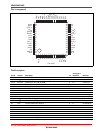
Rev.1.0, Feb.12.2004, page 6 of 29
Internal Functions
Functional Description
• CDS input
CCD low-frequency noise is suppressed by CDS (correlated double sampling).
The signal level is clamped at 14 LSB to 76 LSB by resister during the OB period. *
1
Gain can be adjusted using 8 bits of register (0.132 dB steps) within the range from –2.36 dB to 31.40 dB. *
2
• ADC input
The center level of the input signal is clamped at 512 LSB (Typ).
Gain can be adjusted using 8 bits of register (0.01784 times steps, register settings) within the range from 0.57
times (–4.86 dB) to 5.14 times (14.22 dB). *
2
• Automatic offset calibration of PGA and ADC
• DC offset compensation feedback for CCD and CDS
• Pre-blanking
Digital output is fixed at clamp level
• Digital outputs enable function
Note: 1. It is not covered by warranty when 14LSB settings
2. Full-scale digital output is defined as 0 dB (one time) when 1 V is input.
Operating Description
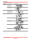
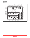
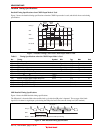
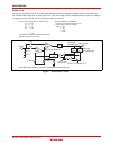
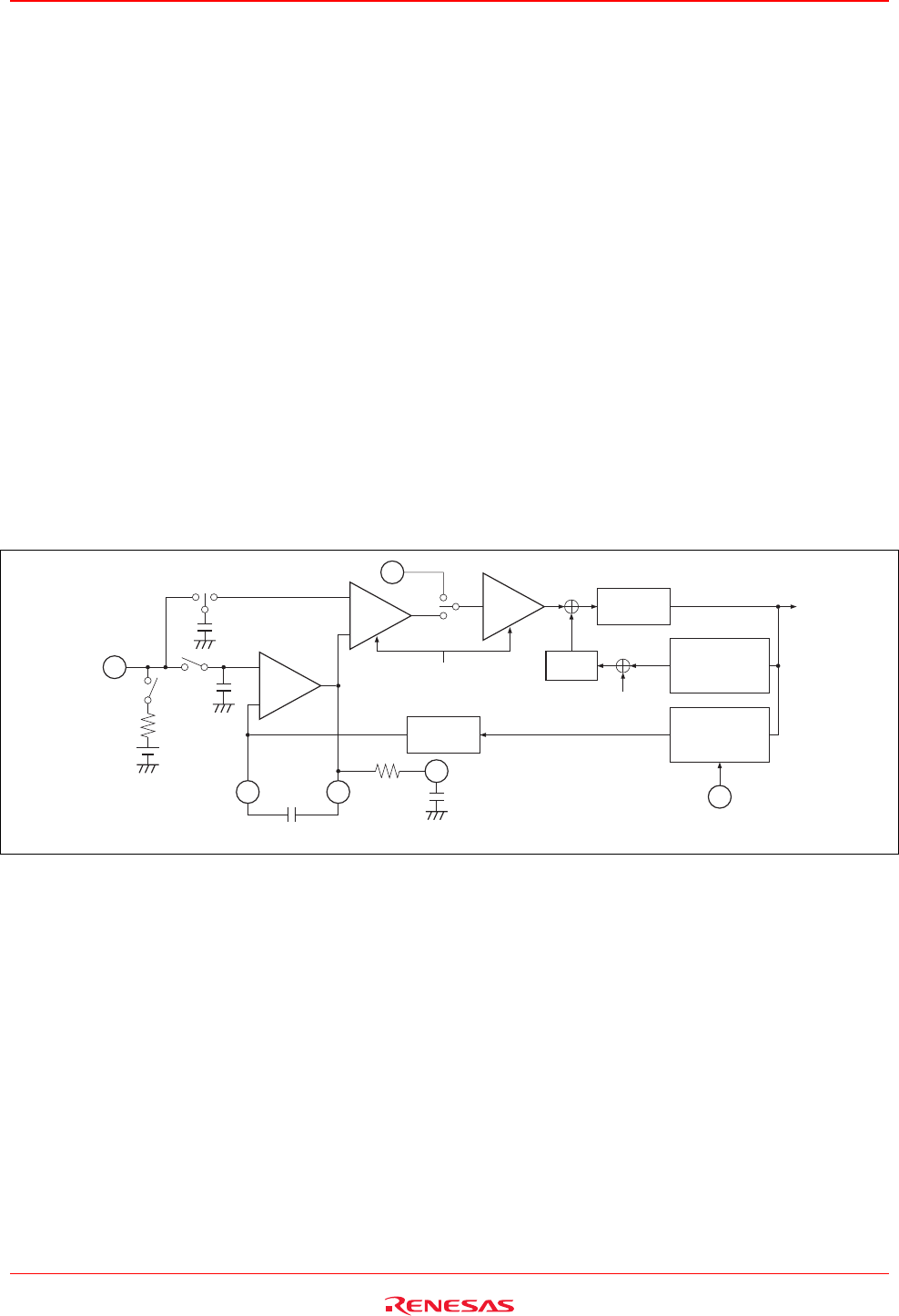
Figure 1 shows CDS/PGA + ADC function block.
DAC
C3
CDS
AMP
PG
AMP
CDS_in
BLKFB
BLKSH
SH
AMP
C2
C1
VRT
SP1
SP1
SP2
10bit
ADC
D0 to D9
BLKC
C4
OBP
ADC_in
Offset
calibration
logic
DC offset
feedback
logic
Gain setting
(register)
Clamp data
(register)
Current
DAC
Figure 1 CDS/PGA Functional Block Diagram
1. CDS (Correlated Double Sampling) Circuit
The CDS circuit extracts the voltage differential between the black level and a signal including the black level. The
black level is directly sampled at C1 by using the SP1 pulse, buffered by the SHAMP, then provided to the
CDSAMP.
The signal level is directly sampled at C2 by using the SP2 pulse, and then provided to CDSAMP (see figure 1).
The difference between these two signal levels is extracted by the CDSAMP, which also operates as a
programmable gain amplifier at the previous stage. The CDS input is biased with VRT (2 V). During the PBLK
period, the above sampling and bias operation are paused.
2. PGA Circuit
The PGAMP is the programmable gain amplifier for the latter stage. The PGAMP and the CDSAMP set the gain
using 8 bits of register.
The equation below shows how the gain changes when register value N is from 0 to 255.
In CDSIN mode: Gain = (–2.36 dB + 0.033 dB) × N (LOG linear).
In ADCIN mode: Gain = (0.57 times + 0.001784 times) × N (linear).
Full-scale digital output is defined as 0 dB (one time) when 1 V is input.