HD49335NP/HNP
Rev.1.0, Feb.12.2004, page 12 of 29
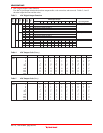
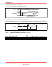
Detailed Timing Specifications at Pre-Blanking
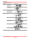
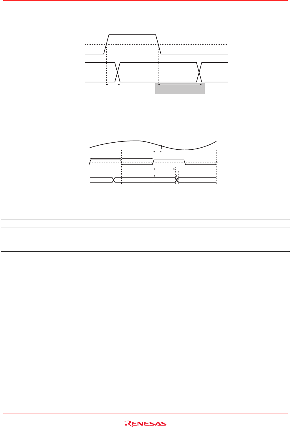
Figure 5 shows the pre-blanking detailed timing specifications.
Digital output
(D0 to D9)
ADC
data
Clamp Level
ADC
data
PBLK
ADCLK × 2 clock ADCLK × 10 clock
Vth
V
OL
V
OH
Figure 5 Detailed Timing Specifications at Pre-Blanking
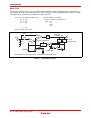
Detailed Timing Specifications when ADCIN Input Mode is Used
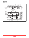
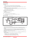
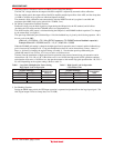
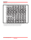
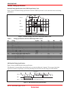
Figure 6 shows the detailed timing chart when ADCIN input mode is used, and table 9 shows each timing specification.
A
DC_in
(1)
A
DCLK
D0 to D9
(2)
Vth
V
DD
/2
(3)
(5)
(4)
Figure 6 Detailed Timing Chart when ADCIN Input Mode is Used
Table 9 Timing Specifications when ADCIN Input Mode is Used
No. Timing Symbol Min Typ Max Unit
(1) Signal fetch time t
ADC1
— (6) — ns
(2), (3) ADCLK t
WH
min./t
WL
min. t
ADC2, 3
Typ × 0.85 1/2f
ADCLK
Typ × 1.15 ns
(4) ADCLK rising to digital output hold time t
AHLD4
— (14.5) — ns
(5) ADCLK rising to digital output delay time t
AOD5
— (23.5) — ns


